Light-emitting diode and method for manufacturing same

a technology of light-emitting diodes and manufacturing methods, which is applied in the direction of basic electric elements, electrical appliances, semiconductor devices, etc., can solve the problems of difficult to improve the electrical and optical properties of light-emitting diodes, the light-emitting diodes of lateral structures tend to suffer from considerable area loss, and the crystal defects of gan layers grown on the sapphire substrate tend to be large, so as to prevent the reduction of light-emitting area, reduce crystal defects

Inactive Publication Date: 2016-03-08
SEOUL VIOSYS CO LTD
View PDF20 Cites 38 Cited by
  • Summary
  • Abstract
  • Description
  • Claims
  • Application Information

AI Technical Summary

Benefits of technology

[0007]The present invention is aimed at providing a light emitting diode that can reduce crystal defects, thereby providing improved luminous efficiency, and a method of fabricating the same.
[0008]In addition, the present invention is aimed at providing a light emitting diode that can prevent reduction in light emitting area, and a method of fabricating the same.
[0009]Further, the present invention is aimed at providing a light emitting diode that can achieve uniform spreading of electric current into an active area, and a method of fabricating the same.
[0016]According to embodiments of the present invention, use of the GaN substrate can or potentially can reduce crystal defects in the first conductive-type semiconductor layer, the active layer, and the second conductive-type semiconductor layer, thereby providing improved luminous efficacy. In addition, the first electrode is electrically connected to the first conductive-type semiconductor layer through the GaN substrate, thereby preventing reduction in light emitting area due to formation of the first electrode. Furthermore, the first electrode is electrically connected to the first conductive-type semiconductor layer via through-holes to allow or potentially allow uniform spreading of electric current in the active area.

Problems solved by technology

However, since the sapphire substrate and GaN layers have large differences in their coefficients of thermal expansion and lattice constants, the GaN layers grown on the sapphire substrate tend to contain many crystal defects such as threading dislocations, and the like.
These crystal defects can make it difficult to improve electrical and optical properties of the light emitting diode.
The light emitting diode of the lateral structure tends to suffer from considerable area loss due to elimination of some portions of an active area for forming electrodes, and substantial light loss caused by the electrodes.
However, the flip-chip type light emitting diode also tend to require elimination of some portions of the active area for forming electrodes, that tend to cause area loss.

Method used


Image

  • Light-emitting diode and method for manufacturing same
  • Light-emitting diode and method for manufacturing same
  • Light-emitting diode and method for manufacturing same

Examples


Embodiment Construction

[0020]Hereinafter, exemplary embodiments of the present invention will be described in detail with reference to the accompanying drawings. It should be understood that the following embodiments are provided for complete disclosure and thorough understanding of the invention by those skilled in the art. Thus, it should be understood that the present invention is not limited to the following embodiments and can be embodied in different ways. In addition, in the drawings, the width, length and thickness of components may be exaggerated for convenience. Further, it should be noted that the drawings are not to precise scale. Like components will be denoted by like reference numerals throughout the specification.

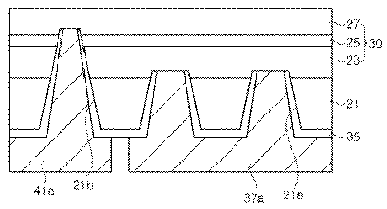
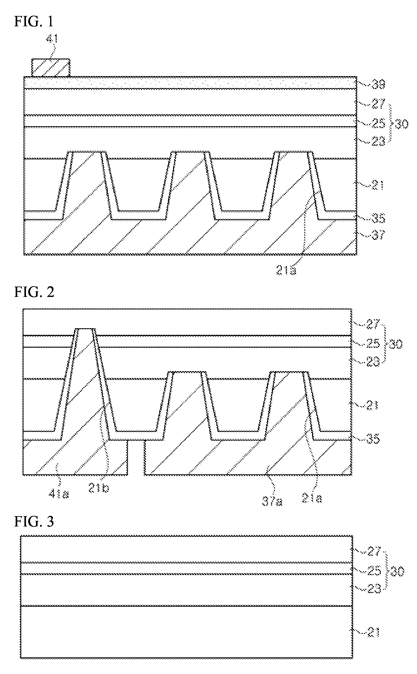
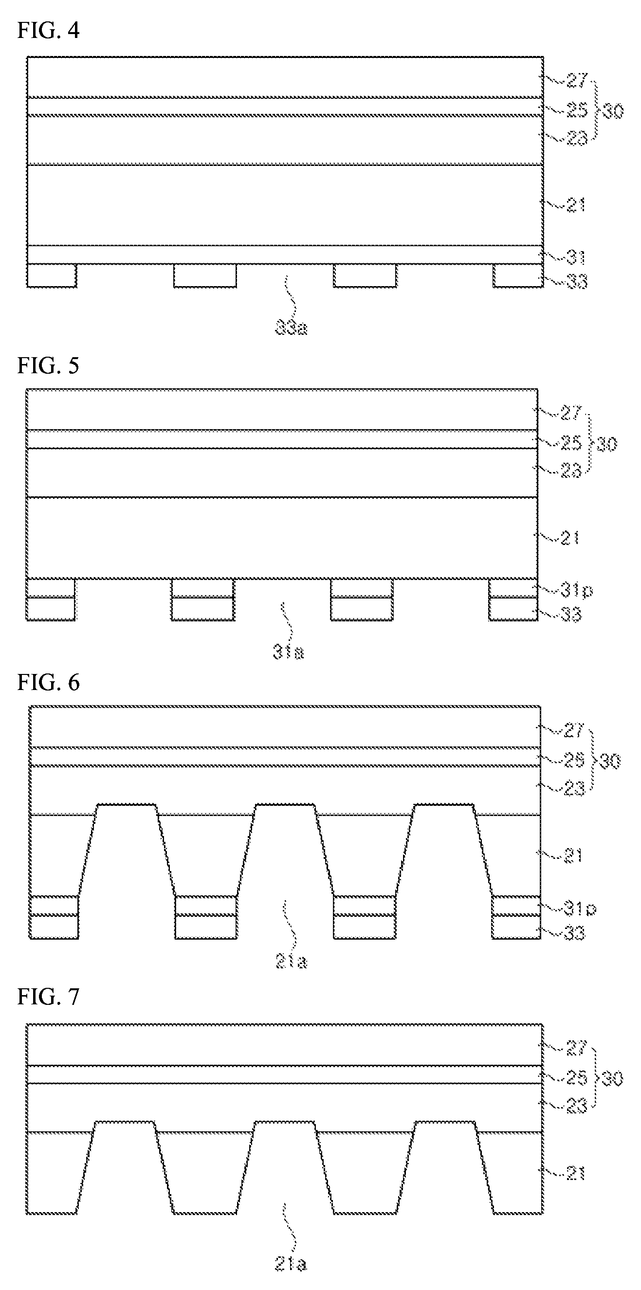
[0021]FIG. 1 is a sectional view of a light emitting diode in accordance with one embodiment of the present invention.

[0022]Referring to FIG. 1, a light emitting diode according to one embodiment of the invention includes a GaN substrate 21, a first conductive-type semiconductor l...


PUM


Abstract

Disclosed are a light emitting diode and a method of fabricating the same. The light emitting diode includes a GaN substrate having a plurality of through-holes; a GaN-based semiconductor stack structure placed on the substrate and including a first conductive-type semiconductor layer, an active layer, and a second conductive-type semiconductor layer; and a first electrode electrically connected to the first conductive-type semiconductor layer via the through-holes. The light emitting diode can reduce crystal defects and prevent reduction in light emitting area.

Description

[0001]This patent document is a 35 U.S.C. 371 National Stage application of PCT Application No. PCT / KR2013 / 001552 entitled “LIGHT-EMITTING DIODE AND METHOD FOR MANUFACTURING SAME,” filed on Feb. 27, 2013, which claims the benefit of priority to Korean Patent Application No. 10-2012-0026240 entitled “LIGHT EMITTING DIODE AND A METHOD FOR MANUFACTURING LIGHT EMITTING DIODE,” filed on Mar. 14, 2012. The entire disclosures of the above applications are incorporated by reference as part of this document.BACKGROUND[0002]1. Field of the Invention[0003]The present invention relates to a light emitting diode (LED) and a method of fabricating the same, and more particularly, to a light emitting diode having a GaN substrate and a method of fabricating the same.[0004]2. Discussion of Related Art[0005]Generally, a light emitting diode can be formed by growing GaN-based semiconductor layers on a sapphire substrate. However, since the sapphire substrate and GaN layers have large differences in the...

Claims


Application Information

Patent Timeline
Patent Type & Authority Patents(United States)
IPC IPC(8): H01L33/38H01L33/24H01L33/00H01L33/06H01L33/10H01L33/32H01L33/42
CPCH01L33/24H01L33/0025H01L33/0075H01L33/06H01L33/10H01L33/32H01L33/382H01L33/42H01L2933/0016H01L2933/0058H01L33/20H01L33/36H01L33/38
Inventor SUH, DUK ILKIM, KYOUNG WANYOON, YEO JINKIM, JI HYE
Owner SEOUL VIOSYS CO LTD
Why Eureka
Try Eureka