Method for manufacturing SOI substrate and method for manufacturing semiconductor device

a technology of semiconductor devices and soi substrates, which is applied in the direction of identification means, instruments, optics, etc., can solve the problems of insufficient recovery of inability to heat treatment at a temperature of 1000° c. or more, and damage to silicon layers by ion irradiation steps, etc., to achieve high reliability, high planarity, and high performance

Inactive Publication Date: 2009-01-01
SEMICON ENERGY LAB CO LTD
View PDF18 Cites 46 Cited by
  • Summary
  • Abstract
  • Description
  • Claims
  • Application Information

AI Technical Summary

Benefits of technology

[0034]By heat treatment by supplying high energy by using at least one kind of particles having the high energy and by polishing treatment, an SOI substrate having a semiconductor layer in which crystal defects are reduced and has high planarity, which is suitable for practical use can be manufactured even when a substrate of whi...

Problems solved by technology

In an ion irradiation step to form an embrittlement layer, a silicon layer is damaged by being irradiated with ions.
However, when a substrate of which heat-resistant temperature is low, such as a glass subst...

Method used


Image

  • Method for manufacturing SOI substrate and method for manufacturing semiconductor device
  • Method for manufacturing SOI substrate and method for manufacturing semiconductor device
  • Method for manufacturing SOI substrate and method for manufacturing semiconductor device

Examples


embodiment mode 1

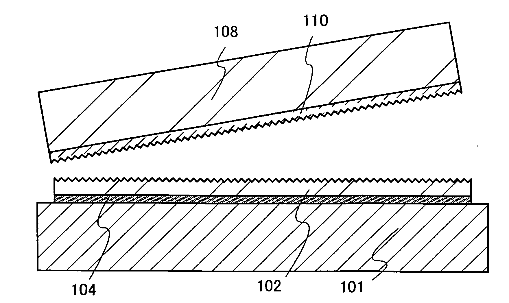
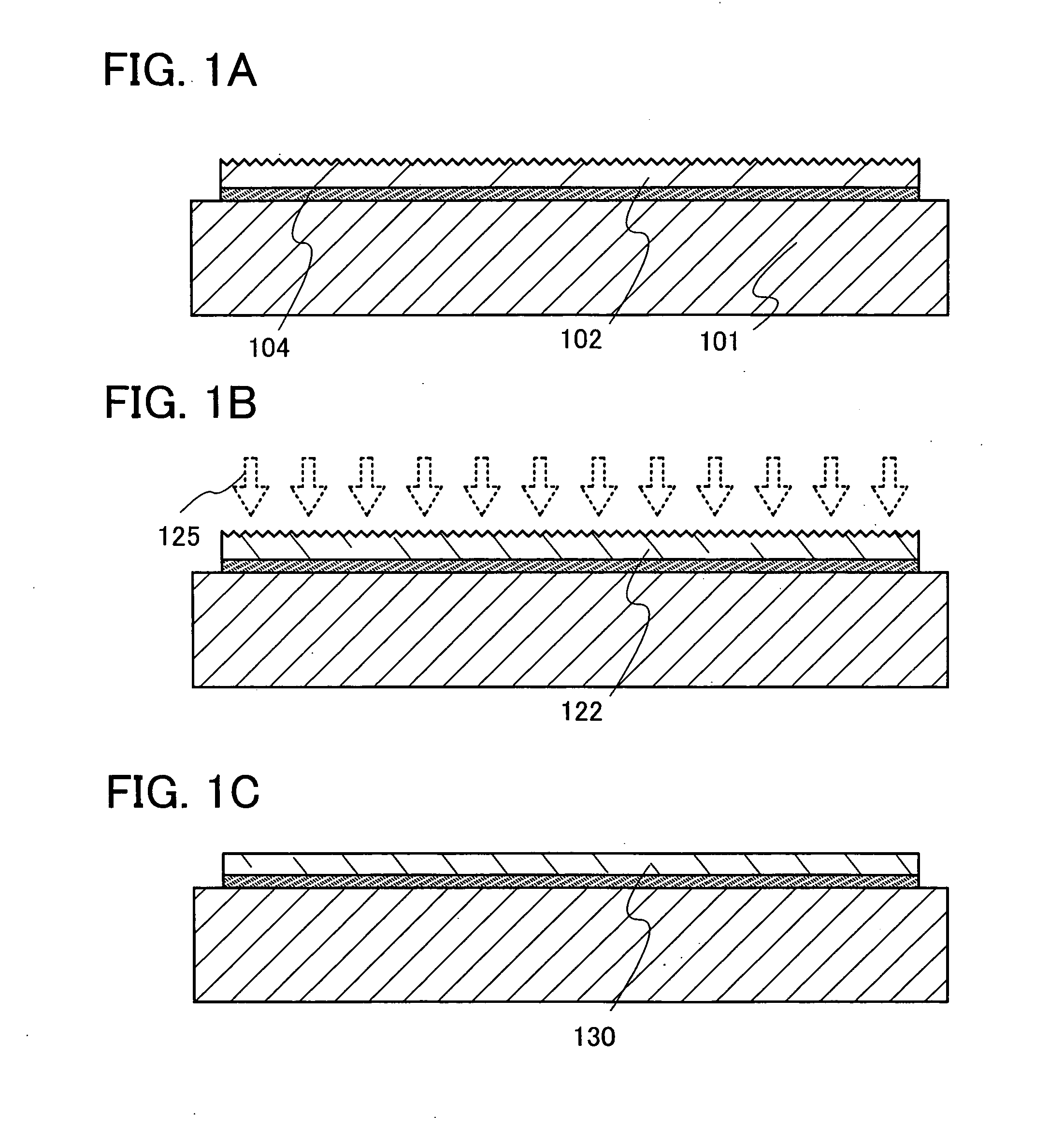
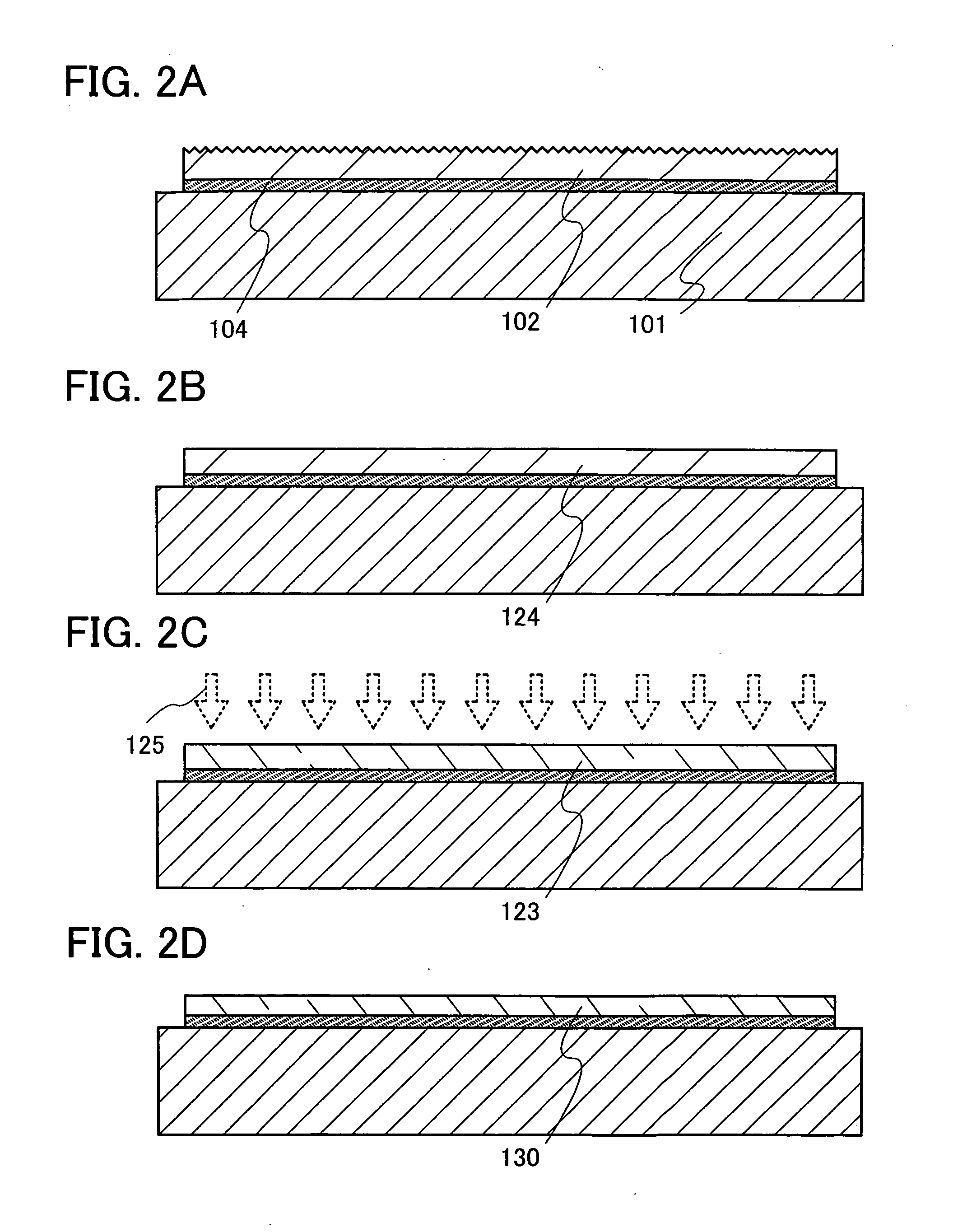
[0057]A method for manufacturing a semiconductor device of the present invention will be described using FIGS. 1A to 1C, FIGS. 2A to 2D, FIGS. 3A to 3D, and FIGS. 4A to 4C.

[0058]In this embodiment mode, a semiconductor layer, which is separated from a semiconductor substrate and bonded to a supporting substrate having an insulating surface, is heated by supplying high energy by using at least one kind of particles having the high energy, and polishing treatment is performed on the heated surface of the semiconductor layer. It is preferable that a single-crystal semiconductor substrate be used as the semiconductor substrate and a single-crystal semiconductor layer be formed as the semiconductor layer which is separated from the semiconductor substrate and bonded to the supporting substrate.

[0059]First, a method for providing the semiconductor layer from the semiconductor substrate over the supporting substrate which is a substrate having an insulating surface will be described using ...

embodiment mode 2

[0124]In this embodiment mode, a method for manufacturing a CMOS (complementary metal oxide semiconductor) will be described as an example of a method for manufacturing a semiconductor device including a semiconductor element having high performance and high reliability with high yield, using FIGS. 5A to 5E and FIGS. 6A to 6D. Note that repetitive description for the same components as or components having similar functions to the components in Embodiment Mode 1 will be omitted.

[0125]In FIG. 5A, the blocking layer 109, the insulating layer 104, the protective layer 121, and the semiconductor layer 130 are formed over the supporting substrate 101. The semiconductor layer 130 corresponds to that shown in FIG. 1C or 2D; and the blocking layer 109, the insulating layer 104, and the protective layer 121 correspond to those shown in FIG. 4C. Note that, although an example in which an SOI substrate having the structure shown in FIG. 5A is used is described in this embodiment mode, an SOI s...

embodiment mode 3

[0152]In this embodiment mode, an example of a method for manufacturing a semiconductor device (also referred to as a liquid crystal display device) having a display function as a semiconductor device having high performance and high reliability with high yield will be described using FIGS. 7A and 7B. Specifically, a liquid crystal display device that includes a liquid crystal display element as a display element will be described.

[0153]FIG. 7A is a top view of a semiconductor device which is one mode of the present invention, and FIG. 7B is a cross-sectional view taken along a line C-D of FIG. 7A.

[0154]As shown in FIG. 7A, a pixel region 306 and driver circuit regions 304a and 304b which are scanning line driver circuits are sealed between a supporting substrate 310 and a counter substrate 395 with a sealant 392. In addition, a driver circuit region 307 which is a signal line driver circuit formed using a driver IC is provided over the supporting substrate 310. A transistor 375 and...


PUM


Abstract

To provide a method for manufacturing an SOI substrate provided with a single-crystal semiconductor layer which is suitable for practical use even when a substrate of which heat-resistant temperature is low, such as a glass substrate, is used, and to manufacture a highly reliable semiconductor device using such an SOI substrate. A semiconductor layer, which is separated from a semiconductor substrate and bonded to a supporting substrate having an insulating surface, is heated by supplying high energy by using at least one kind of particles having the high energy, and polishing treatment is performed on the heated surface of the semiconductor layer. At least part of a region of the semiconductor layer can be melted by the heat treatment by supplying high energy to reduce crystal defects in the semiconductor layer. Further, the surface of the semiconductor layer can be polished and planarized by the polishing treatment.

Description

BACKGROUND OF THE INVENTION[0001]1. Field of the Invention[0002]The present invention relates to a method for manufacturing an SOI substrate having a so-called SOI (silicon on insulator) structure in which a semiconductor layer is provided on an insulating surface and a method for manufacturing a semiconductor device having an SOI structure.[0003]2. Description of the Related Art[0004]As an alternative to an integrated circuit using a silicon wafer which is manufactured by thinly slicing an ingot of a single-crystal semiconductor, an integrated circuit using a semiconductor substrate which is referred to as a silicon-on-insulator (hereinafter also referred to as ‘SOI’) substrate, in which a thin single-crystal semiconductor layer is provided on an insulating surface has been developed. The integrated circuit using an SOI substrate has attracted attention as an integrated circuit which reduces parasitic capacitance between a drain and a substrate of a transistor and improves the perf...

Claims


Application Information

Patent Timeline
IPC IPC(8): H01L21/782H01L33/00H01L21/00H01L21/30H01L21/46G02F1/1368G09F9/30H01L21/02H01L21/20H01L21/265H01L21/322H01L21/336H01L27/12H01L29/786H01L51/50H05B33/02H05B33/14
CPCH01L21/31612H01L21/76254H01L29/66772H01L27/1266H01L27/1214H01L21/02211H01L21/02271H01L21/02164
Inventor OHNUMA, HIDETOIMAHAYASHI, RYOTAIIKUBO, YOICHIMAKINO, KENICHIRONAGAMATSU, SHO
Owner SEMICON ENERGY LAB CO LTD
Why Eureka
Try Eureka