

Method for heat treatment of silicon wafers and silicon wafer
a technology of heat treatment and silicon wafers, applied in the field of heat treatment of silicon wafers, can solve the problems of affecting the carrier mobility directly under the gate oxide film, the dielectric breakdown of the oxide film, and the deformation of the electric characteristic of the wafer, so as to reduce the crystal defects of the wafer surface layer, without degrading the microroughness
- Summary
- Abstract
- Description
- Claims
- Application Information
AI Technical Summary
Benefits of technology
Problems solved by technology
Method used
Image

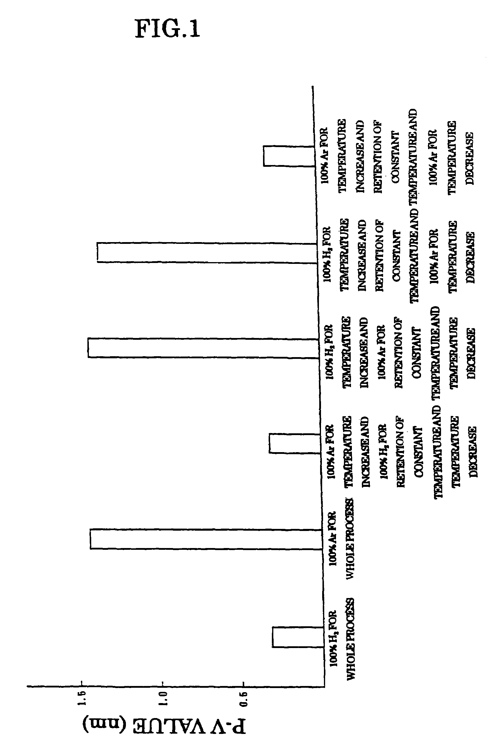
Examples
example 2
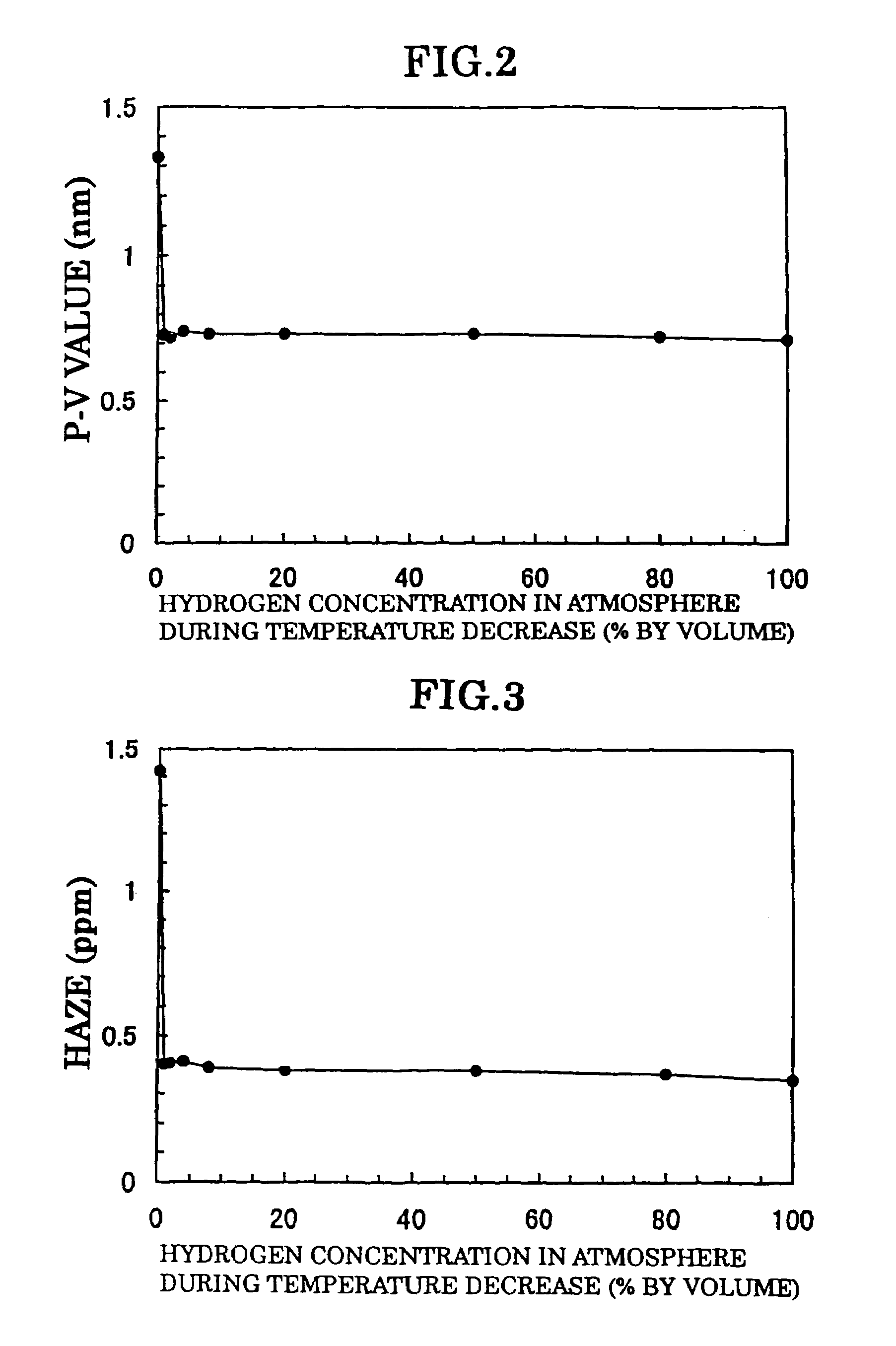
[0123]A silicon wafer obtained by the Czochralski method was subjected to a heat treatment using an RTA apparatus at 1200° C. for 10 seconds under 100% hydrogen atmosphere. The temperature decreasing rate during temperature decreasing from the maximum temperature of the heat treatment was 20° C. / sec according to the method of present invention. Haze on the surface of the silicon wafer was measured after the heat treatment.
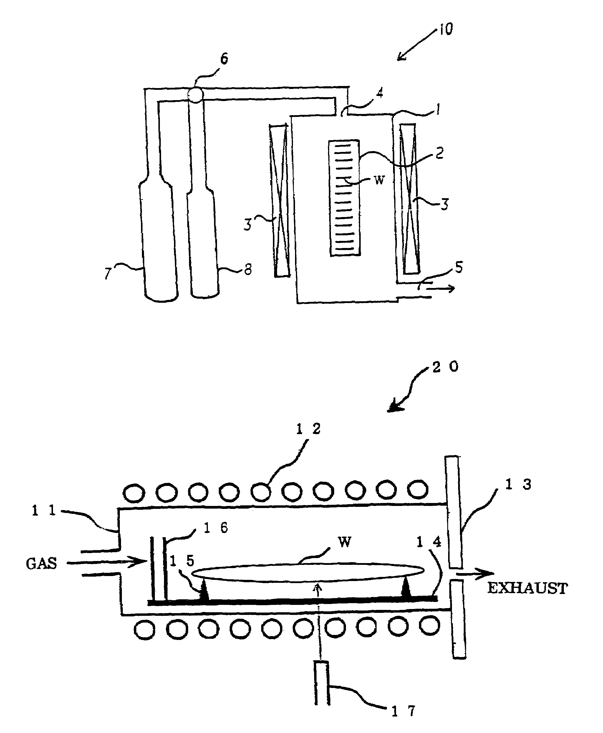
[0124]For the heat treatment, the aforementioned RTA apparatus (rapid heating and rapid cooling apparatus Model SHS-2800, Steag Microtec International) was used.
[0125]The silicon wafer-used was one obtained by slicing a silicon ingot manufactured by the Czochralski method and subjecting the sliced wafer to mirror polishing in a usual manner, and having a diameter of 6 inches and crystal orientation of .
[0126]Haze was measured by using a particle counter, LS-6030 (tradename of Hitachi Electronics Engineering Co., Ltd.) in a measurement voltage 700V range. The haze l...
example 3
[0128]A silicon wafer was subjected to a heat treatment in the same manner as Example 2, except that a temperature decreasing rate of 5° C. / sec for the region of from the maximum temperature of 1200° C. to 700° C. and a temperature decreasing rate of 60° C. / sec for the region below 700° C. were used. The heat treatment and the haze measurement were performed in the same manner as Example 2 except for the aforementioned modifications.
[0129]As a result of the measurement, the wafer of Example 3 was found to have a haze level of about 25 bits, which is markedly improved and well meets to higher integration degree in future.
PUM
| Property | Measurement | Unit |
|---|---|---|
| surface roughness | aaaaa | aaaaa |
| surface roughness | aaaaa | aaaaa |
| temperature | aaaaa | aaaaa |
Abstract
Description
Claims
Application Information