Bandpass filter, high-frequency device and communications apparatus

a filter and high-frequency technology, applied in the field of bandpass filters, can solve the problem that the resonance capacitance does not have a sufficiently short-circuiting impedance at high frequencies, and achieve the effects of reducing interlayer electromagnetic coupling, reducing coupling, and suppressing variation of characteristics due to the lateral displacement of lamination

Active Publication Date: 2016-03-15
HITACHI METALS LTD
View PDF25 Cites 8 Cited by
  • Summary
  • Abstract
  • Description
  • Claims
  • Application Information

AI Technical Summary

Benefits of technology

[0008]The second object of the present invention is to provide a bandpass filter that can be miniaturized with low loss, a high-frequency device comprising it, and a communications apparatus.DISCLOSURE OF THE INVENTION
[0021]Said bandpass filter preferably comprises coupling capacitance for coupling pluralities of resonance lines, said coupling capacitance being constituted by pluralities of opposing capacitance electrodes connected to the resonance lines to be coupled, and pluralities of said capacitance electrodes being formed on different dielectric layers from those on which said resonance lines are formed, via said ground electrode. This structure enables coupling capacitance to be formed with a high freedom of design, without restriction by narrow intervals of the resonance lines.

Problems solved by technology

However, when via-conductors have large parasitic inductance, the resonance capacitances do not have sufficiently short-circuiting impedance at high frequencies.

Method used


Image

  • Bandpass filter, high-frequency device and communications apparatus
  • Bandpass filter, high-frequency device and communications apparatus
  • Bandpass filter, high-frequency device and communications apparatus

Examples


Embodiment Construction

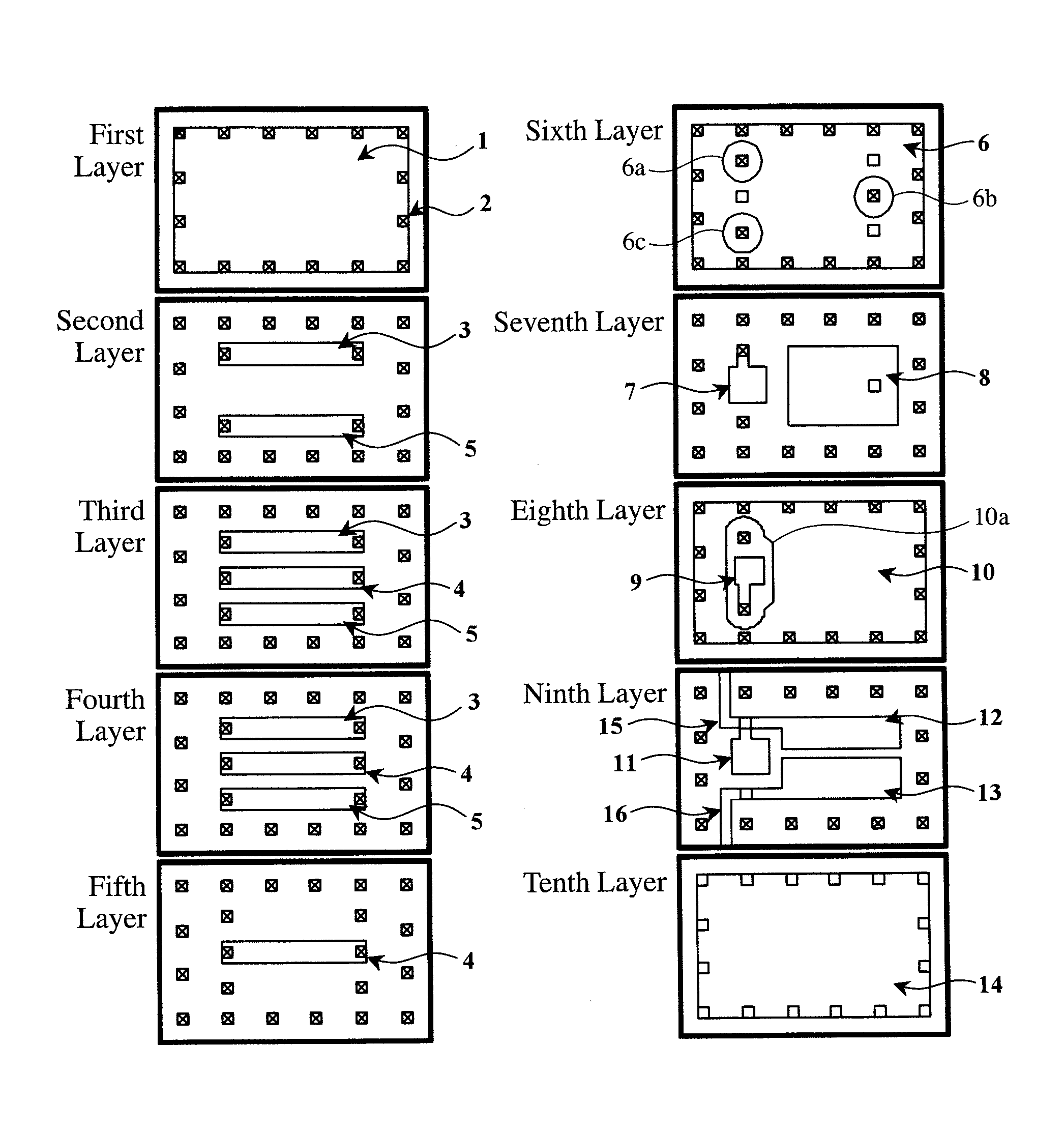
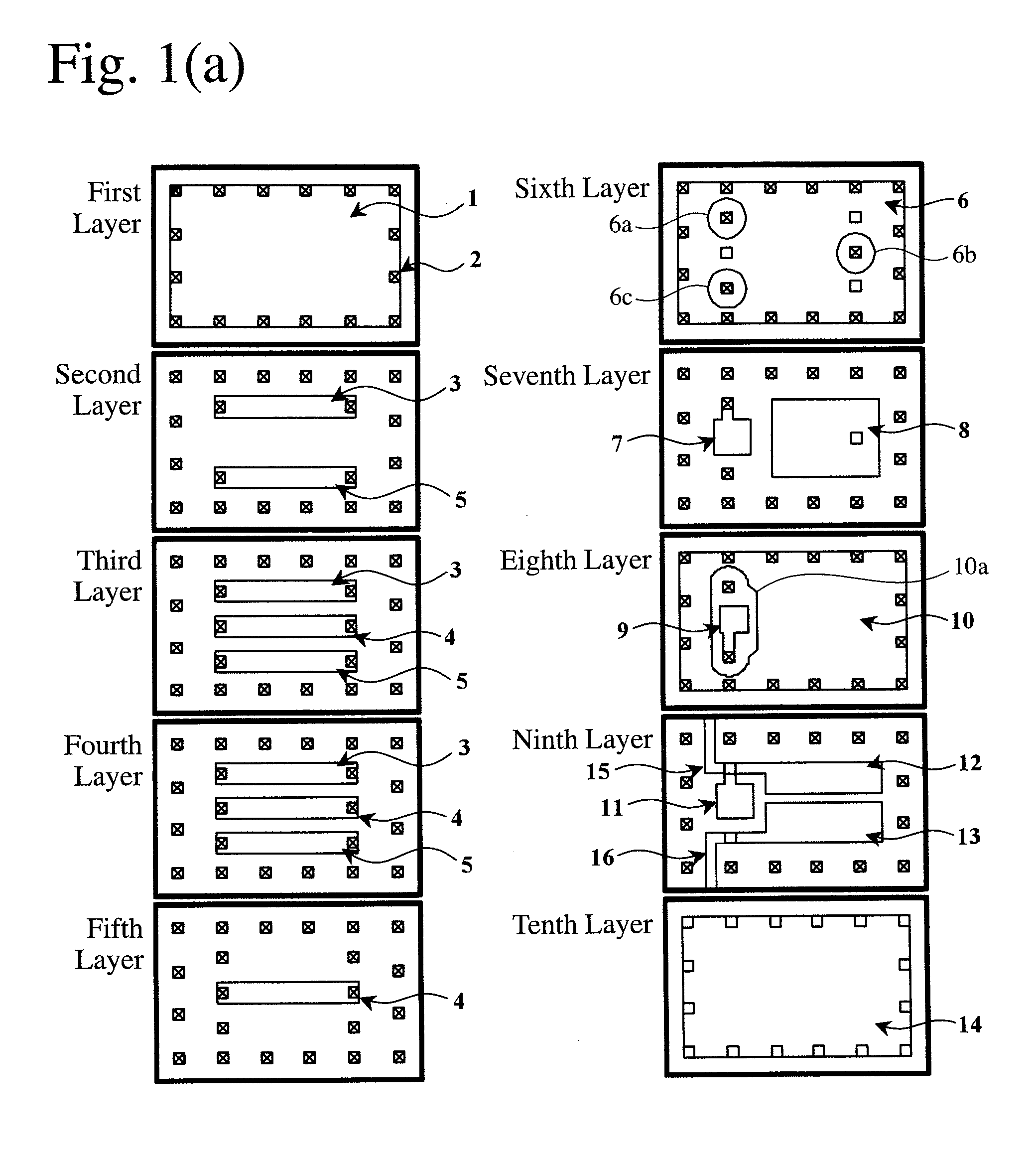
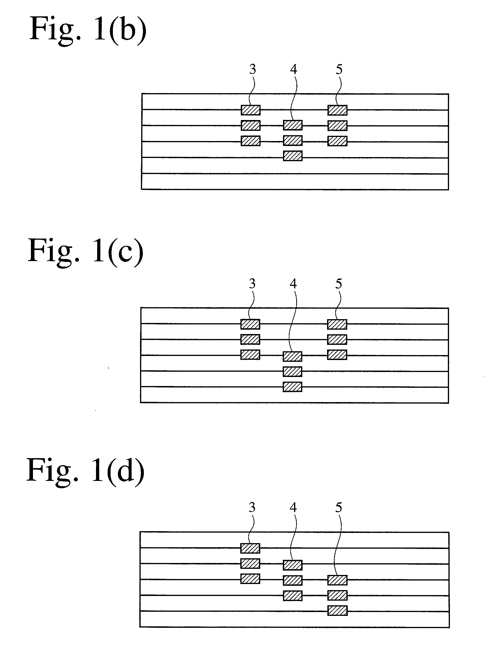
[0040]Each embodiment of the present invention will be explained in detail below referring to the attached drawings without intention of restricting the present invention thereto, and the explanation of each embodiment is applicable to other embodiments unless otherwise mentioned. The bandpass filter of the present invention is a laminate-type bandpass filter constituted by a laminate substrate comprising pluralities of dielectric layers provided with conductor patterns, which comprises two or more resonators between two input / output terminals. Each resonator is constituted, for example, by a resonance line and a resonance capacitance connected to one end of the resonance line.

[0041]FIG. 1(a) shows conductor patterns on each layer constituting a laminate-type bandpass filter according to an embodiment of the present invention, and FIG. 2 shows one example of the equivalent circuits of the bandpass filter shown in FIG. 1(a). This bandpass filter comprises three resonators each consti...


PUM


Abstract

A bandpass filter comprising two or more resonators arranged between two input / output terminals in a laminate substrate comprising pluralities of dielectric layers; each resonator being constituted by a resonance line and a resonance capacitance connected to one end of the resonance line; capacitance electrodes forming said resonance capacitances and said resonance lines being arranged on different dielectric layers, via a planar ground electrode covering the entire structural portion of the bandpass filter when viewed in a lamination direction; and in each of the resonators connected to said two input / output terminals, the junctions of said input / output terminals to said paths between said resonance lines and said resonance capacitances being closer to said resonance capacitances than said resonance lines in a lamination direction.

Description

[0001]This is a National Stage of International Application No. PCT / JP2009 / 064050 filed Aug. 7, 2009, claiming priority based on Japanese Patent Application Nos. 2008-206667 and 2008-206668 filed Aug. 11, 2008 and 2008-220320 filed Aug. 28, 2008, respectively, the contents of all of which are incorporated herein by reference in their entirety.FIELD OF THE INVENTION[0002]The present invention relates to a bandpass filter used in, for example, mobile communications appliances such as cell phones, wireless communications apparatuses such as wireless LAN for wireless transmission between electronic / electric equipments, etc., and a high-frequency device and a communications apparatus comprising such bandpass filter.BACKGROUND OF THE INVENTION[0003]Data communications by wireless LAN such as IEEE802.11 are now widely used. The wireless LAN is used, for instance, in personal computers (PCs), PC peripherals such as printers and hard disk drives, electronic equipments such as FAXs, standard ...

Claims


Application Information

Patent Timeline
Patent Type & Authority Patents(United States)
IPC IPC(8): H03H7/09H03H7/01H01P1/203H01P1/213H03H1/00
CPCH03H7/0123H01P1/20345H01P1/2135H03H7/09H03H2001/0085H01P1/20H03H7/12
Inventor FUKAMACHI, KEISUKEYAMASHITA, TAKAHIROUMEYAMA, TAKAHIRO
Owner HITACHI METALS LTD
Why Eureka
Try Eureka