High-frequency module

a high-frequency module and module technology, applied in the field of high-frequency modules, can solve the problems of reducing the reception sensitivity and distortion of transmission signals, affecting the harmonic noise of affecting the transmission of transmission signals, so as to reduce the influence of harmonic noise due to input of high-frequency switch control signals, the effect of reducing the degradation of communication characteristics

Active Publication Date: 2016-03-29
MURATA MFG CO LTD
View PDF25 Cites 5 Cited by
  • Summary
  • Abstract
  • Description
  • Claims
  • Application Information

AI Technical Summary

Benefits of technology

[0008]In view of the above situation, preferred embodiments of the present invention provide a high-frequency module in which degradation in communication characteristics has been reduced by reducing the influence of harmonic noise due to high-frequency switch control signals.
[0020]According to various preferred embodiments of the present invention, electromagnetic coupling between the control signal wiring conductor and the high-frequency signal wiring conductor and electromagnetic coupling between the control signal wiring conductor and the matching device conduction ground conductor are suppressed or prevented, such that the influence of harmonic noise due to input of a high-frequency switch control signal is significantly reduced. As a result, degradation of the communication characteristics, such as a decrease in reception sensitivity and distortion of a transmission signal, is significantly reduced.

Problems solved by technology

Further, when an electronic component other than the high-frequency switch is provided, harmonic noise due to the high-frequency switch control signals is superimposed on a ground conductor that is electrically connected to the electronic component through a ground conductor layer within the multilayer substrate, and the superimposition is caused by the fact that the ground conductor (matching device conduction ground conductor) electrically connected to the electronic component is close to the control signal wiring conductor.

Method used


Image

  • High-frequency module
  • High-frequency module
  • High-frequency module

Examples


first preferred embodiment

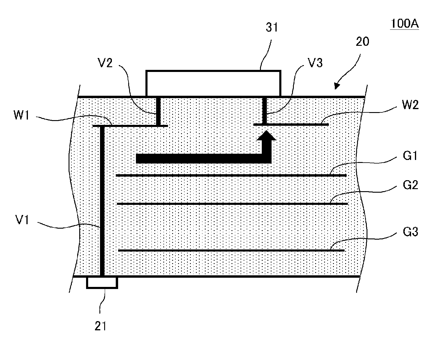
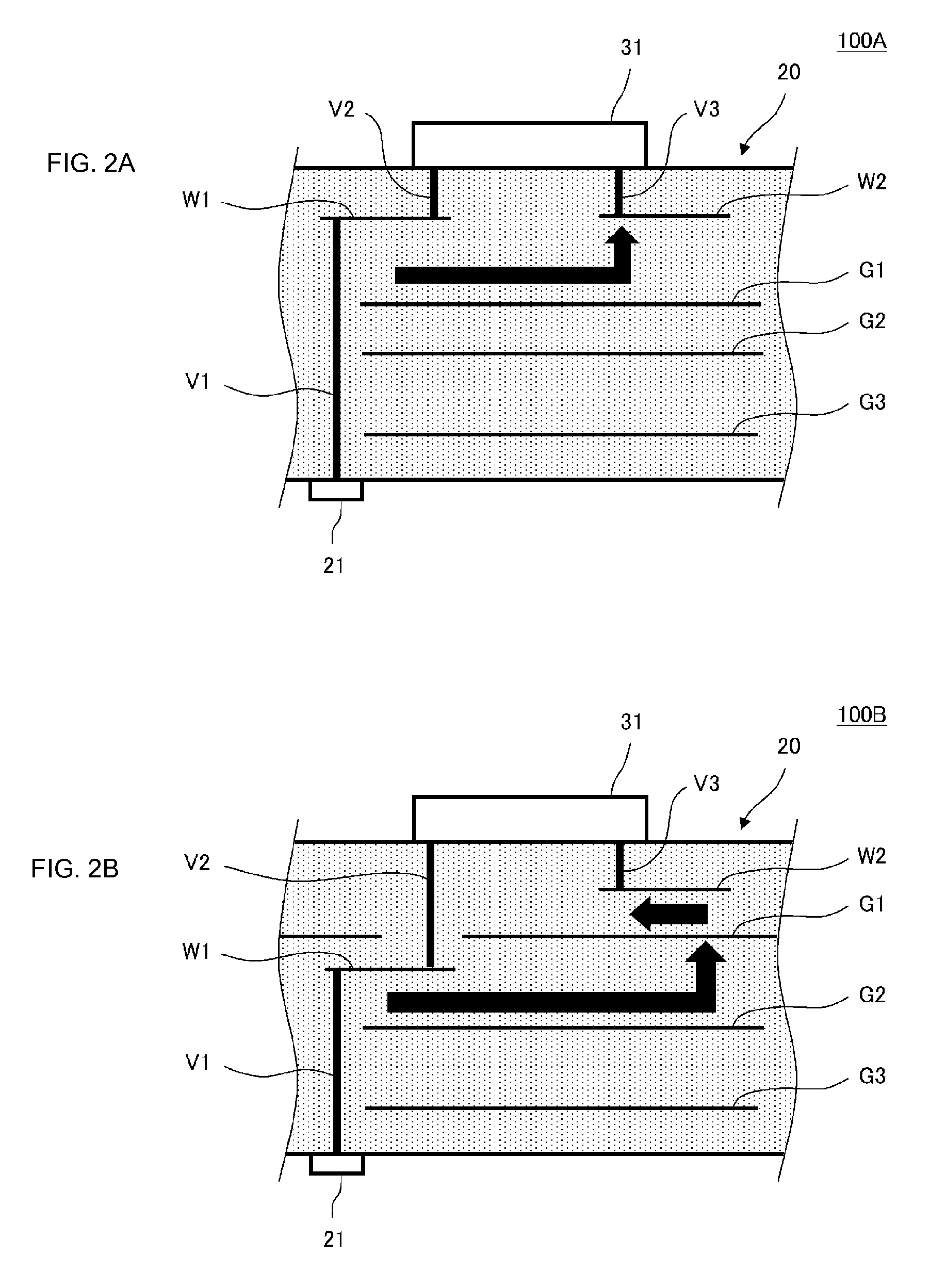
[0033]FIG. 2A and FIG. 2B are sectional views of the major portions of high-frequency modules 100A and 100B, which are comparative examples (based on existing general design methods) of a high-frequency module of a first preferred embodiment of the present invention. FIG. 3 is sectional view of the major portions of a high-frequency module 101 of the first preferred embodiment.

[0034]In FIG. 2A, FIG. 2B, and FIG. 3, the high-frequency modules (100A, 100B, and 101) each include a multilayer ceramic substrate (hereinafter, simply called a “multilayer substrate”) and a high-frequency switch 31 mounted on a first main surface (top surface) of the multilayer substrate 20. The multilayer substrate 20 includes therein wiring conductors W1 and W2, ground conductors G1, G2, and G3, and interlayer connection conductors V1, V2, and V3. A control signal input terminal 21 is located on the second main surface (bottom surface) of the multilayer substrate 20.

[0035]Respective electrodes on which the...

second preferred embodiment

[0042]FIG. 4 is a block configuration diagram of a high-frequency module 102 of a second preferred embodiment of the present invention.

[0043]The high-frequency module 102 of the second preferred embodiment includes a multilayer substrate and includes a high-frequency switch 31, duplexers 32a to 32d, a diplexer 35, filters 34e and 34f, matching inductors La, Lb, Lc, and Ld, and the like mounted on the multilayer substrate. The high-frequency switch 31 includes an antenna port ANT, input / output ports P1 to P7, a power supply terminal Vdd, a ground terminal GND, a serial data input terminal SDATA, a clock signal input terminal SCLK, and a digital circuit portion power supply terminal Vio.

[0044]FIG. 5 is a waveform diagram illustrating a serial data signal S(SDATA) input to the serial data input terminal SDATA and a clock signal S(SCLK) input to the clock signal input terminal SCLK. The high-frequency switch 31 reads predetermined bits of data from serial data in synchronization with th...

third preferred embodiment

[0055]FIG. 7A is a sectional view of the major portions of a high-frequency module 103 of a third preferred embodiment of the present invention, and FIG. 7B is a sectional view of the major portions of a high-frequency module 100D having an existing configuration as a comparative example of the high-frequency module 103.

[0056]In FIGS. 7A and 7B, the high-frequency module (103, 100D) each include a multilayer substrate 20 and include a high-frequency switch 31, an electronic component 36, and the like which are mounted on a first main surface (top surface) of the multilayer substrate 20. The multilayer substrate 20 includes therein wiring conductors W1 to W3, ground conductors G1 to G3, and interlayer connection conductors V1 to V6. A control signal input terminal 21 is located on the second main surface (bottom surface) of the multilayer substrate 20.

[0057]Respective electrodes on which the high-frequency switch 31 is mounted are electrically connected to the wiring conductors W1 an...


PUM


Abstract

A multilayer substrate includes therein wiring conductors, ground conductors, interlayer connection conductors, and a matching inductor. A control signal input terminal is provided on a second main surface of the multilayer substrate. Electrodes on which a high-frequency switch is mounted are electrically connected to the wiring conductors through the interlayer connection conductors. The control signal wiring conductor is located on a dielectric layer close to the second main surface of the multilayer substrate, and the high-frequency signal wiring conductor is located on a dielectric layer close to a first main surface of the multilayer substrate. The ground conductor, which is superposed with the control signal wiring conductor in plan view is separated from the matching device conduction ground conductor by a separation portion. With this structure, influence of harmonic noise due to input of high-frequency switch control signals is reduced and degradation of the communication characteristics is reduced.

Description

BACKGROUND OF THE INVENTION[0001]1. Field of the Invention[0002]The present invention relates to high-frequency modules having a configuration in which a high-frequency switch and a high-frequency filter are mounted on a multilayer substrate, and specifically to high-frequency modules including a control signal input terminal to which a control signal for a high-frequency switch is input.[0003]2. Description of the Related Art[0004]In general, a front-end module is provided between an antenna and a transmitter / receiver circuit in a communication apparatus that performs communication by switching among a plurality of communication frequency bands. For example, Japanese Unexamined Patent Application Publication No. 2004-517583 discloses a front-end module including a high-frequency switch.[0005]FIG. 1 is a circuit diagram of the front-end module illustrated in FIG. 1 of Japanese Unexamined Patent Application Publication No. 2004-517583. In this front-end module, transmission signal in...

Claims


Application Information

Patent Timeline
Patent Type & Authority Patents(United States)
IPC IPC(8): H01P1/10H04B1/00H05K1/02H05K1/16H01P1/213H04B15/00
CPCH01P1/10H01P1/2135H04B1/0057H04B15/00H05K1/0225H05K1/0243H05K1/165
Inventor ONO, ATSUSHI
Owner MURATA MFG CO LTD
Why Eureka
Try Eureka