
Apparatus for producing polycrystalline silicon

a technology of polycrystalline silicon and producing rods, which is applied in the direction of chemistry apparatus and processes, silicon compounds, coatings, etc., can solve the problems of large amount of heat carried away by cooling water from a reactor, inability to reuse heat recovered by cooling water, and low temperature of cooling water, so as to prevent contamination of impurities of polycrystalline silicon and reduce thermal loss

Active Publication Date: 2016-04-19
HIGH-PURITY SILICON CORP
View PDF27 Cites 0 Cited by
  • Summary
  • Abstract
  • Description
  • Claims
  • Application Information

AI Technical Summary

Benefits of technology

The present invention is an apparatus for producing polycrystalline silicon which prevents contamination and ensures high efficiency in recovery of heat through the use of two-phase flow of water and steam as a cooling medium. The recovered heat can also be directly used in factories that require steam, reducing thermal loss.

Problems solved by technology

As a result, large amount of heat is carried away by cooling water from a reactor.
Also, the temperature of the cooling water is low, so that the heat recovered by the cooling water cannot be reused, and generally released from a cooling tower and the like to the environment.
Therefore, it causes great loss of energy, and increases the cost of polycrystalline silicon and the environmental burden.
However, no measure to prevent this problem is mentioned at all in this patent.
In this case, however, the temperature at the inner wall of the reactor becomes high, so that the purity of polycrystalline silicon is deteriorated.
On the other hand, if sending down the temperature of the cooling medium in order to maintain the purity of polycrystalline silicon, the exhaust heat cannot be used because of its low temperature.

Method used


Image

  • Apparatus for producing polycrystalline silicon
  • Apparatus for producing polycrystalline silicon
  • Apparatus for producing polycrystalline silicon

Examples


Embodiment Construction

[0038]Hereinafter, an embodiment of an apparatus for producing polycrystalline silicon according to the present invention will be described with reference to the drawings.

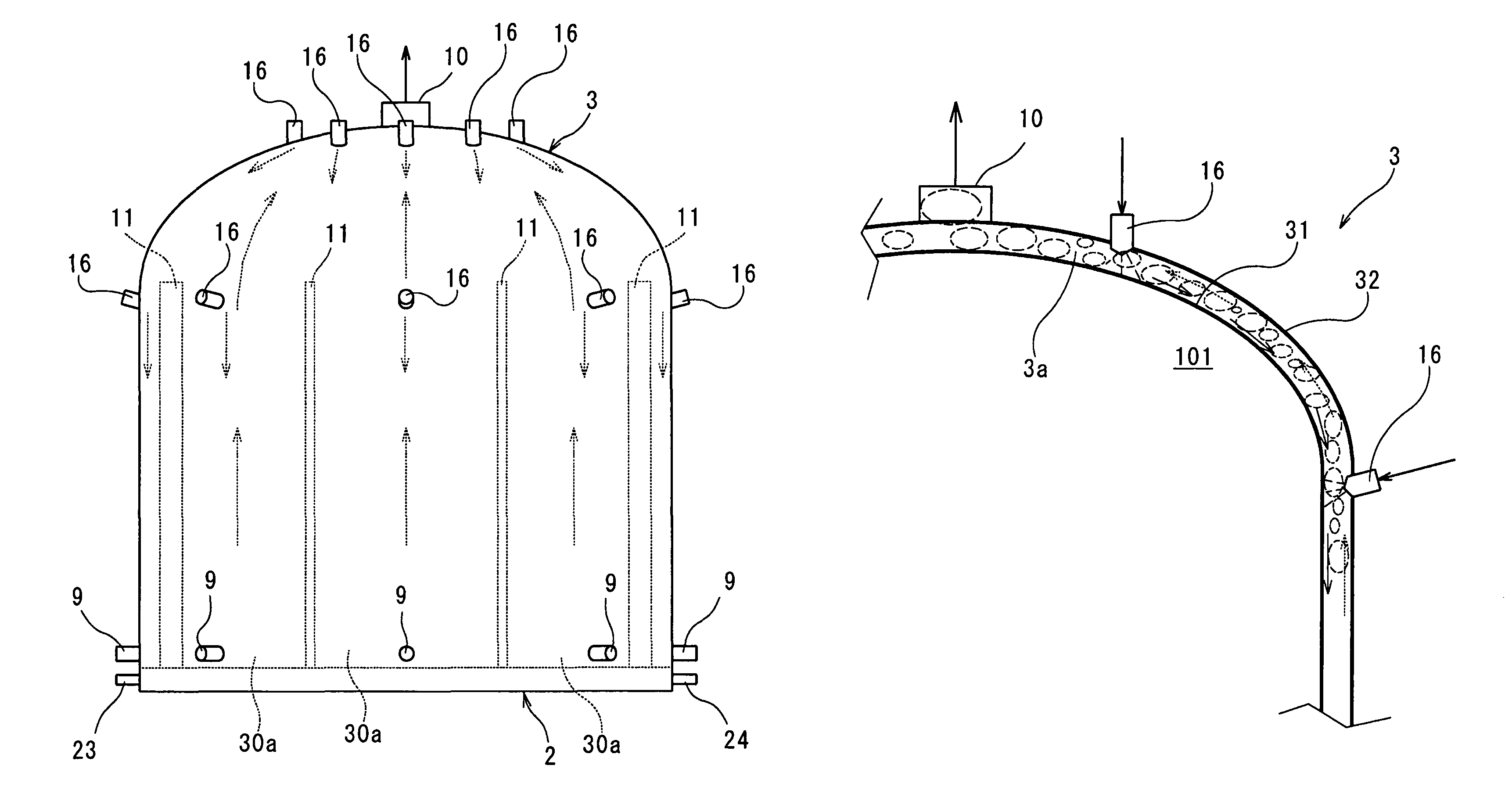
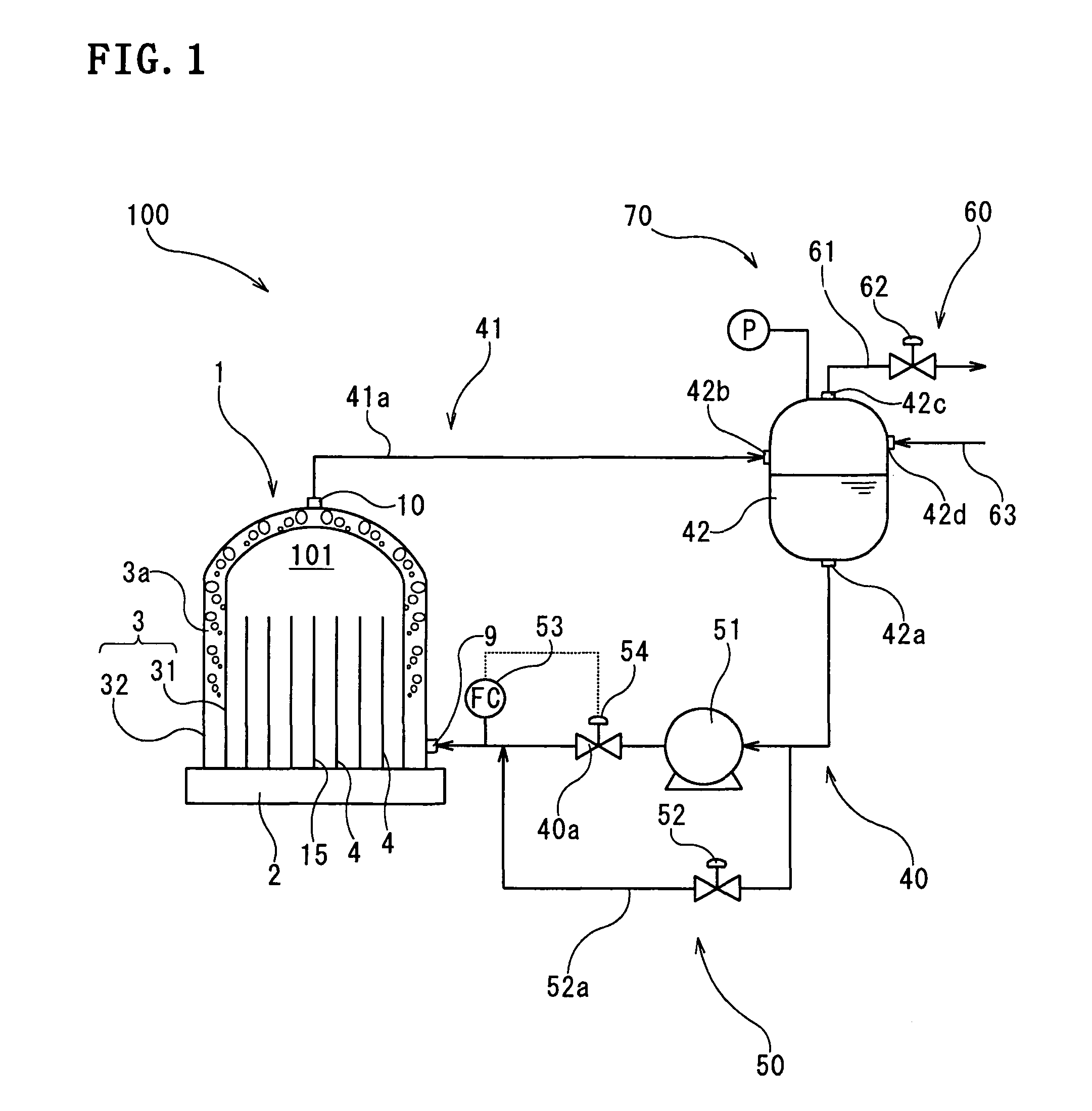
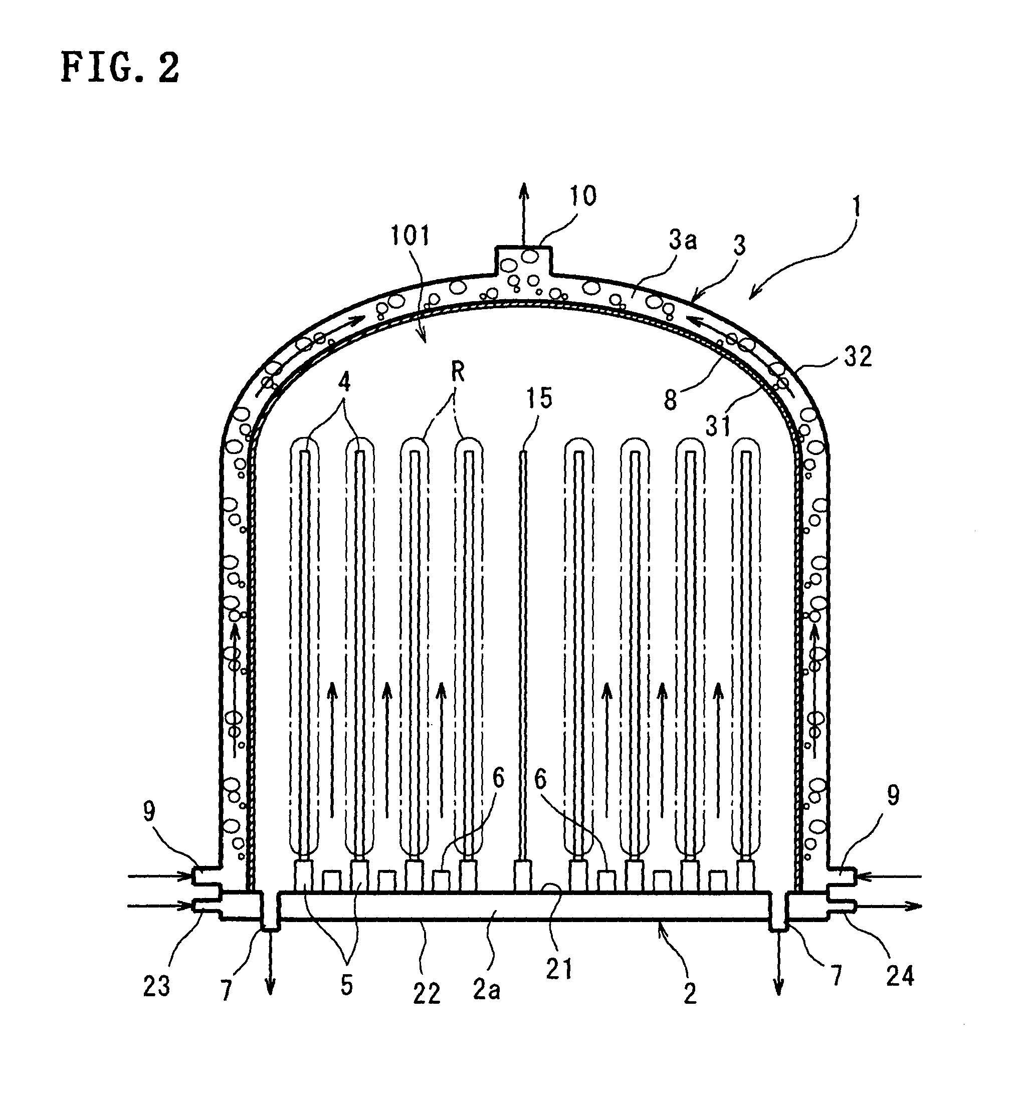
[0039]An apparatus for producing polycrystalline silicon 100 of the present invention is provided with: a reactor 1 having a base 2 forming a reactor floor, and a bell jar 3 which is mounted on the base 2; a coolant feeding system 40 which is connected to the bell jar 3 and supplies cooling medium to a cooling path (space part) 3a of the reactor 1; a coolant recovering system 41 which is connected to the bell jar 3 and recovers the cooling medium from the cooling path 3a; a pressure control part 70 which controls a pressure in the cooling path 3a; and a flow-rate control part 50 which controls a flow rate of the cooling medium being supplied to the cooling path 3a. In the apparatus 100, the cooling medium can be circulated as boiling two-phase flow in the cooling path 3a by controlling the pressure and the flow rat...


PUM

PropertyMeasurementUnit
thermal conductivityaaaaaaaaaa
temperatureaaaaaaaaaa

Abstract

An apparatus for producing polycrystalline silicon having: a bell jar having a circumferential wall forming a chamber of a reactor and a jacket covering a circumferential wall, and in which a cooling path formed between the circumferential wall and the jacket that allows cooling medium including water to flow therethrough; a coolant feeding system which is connected to the bell jar so as to feed the cooling medium to the cooling path; a coolant recovering system which is connected to the bell jar so as to recover the cooling medium from the cooling path; a pressure control part controlling a pressure in the cooling path; and a flow-rate control part controlling a flow rate of the cooling medium, wherein the cooling medium flows in the cooling path as boiling two-phase flow by controlling the pressure and flow rate of the cooling medium.

Description

BACKGROUND OF THE INVENTION[0001]1. Field of the Invention[0002]The present invention is relates to an apparatus for producing polycrystalline silicon producing rods of polycrystalline silicon by depositing polycrystalline silicon on a surface of heated silicon rod in a reactor.[0003]Priority is claimed on Japanese Patent Application No. 2010-108472, filed on May 10, 2010, the content of which is incorporated herein by reference.[0004]2. Description of the Related Art[0005]A producing apparatus by the Siemens process is known as a producing apparatus of polycrystalline silicon. In the producing apparatus of polycrystalline silicon, a plurality of silicon seed rods are vertically set in a reactor and electric current is supplied to heat these rods. Raw gas including silicon compounds, such as chlorosilanes, and hydrogen is supplied into the reactor so as to bring the raw gas into contact with the heated silicon seed rods. As a result, polycrystalline silicon is deposited on the silic...

Claims


Application Information

Patent Timeline
Patent Type & Authority Patents(United States)
IPC IPC(8): C23C16/24C23C16/44C01B33/035
CPCC23C16/24C01B33/035C23C16/4411B01J2219/00085B01J2219/00094
Inventor MIYAZAWA, TAKASHISAIKI, WATARU
Owner HIGH-PURITY SILICON CORP
Learn More