Envelope detector circuit

a detector circuit and envelope technology, applied in the field of envelope detector circuits, can solve the problems of poor sensitivity, inability to operate with low signal amplitude, variations in manufacturing process, etc., and achieve the effects of low power consumption, reduced construction cost, and high sensitivity

Active Publication Date: 2016-06-07
EM MICROELECTRONIC-MARIN
View PDF5 Cites 5 Cited by
  • Summary
  • Abstract
  • Description
  • Claims
  • Application Information

AI Technical Summary

Benefits of technology

[0008]It is an aim of the present invention to overcome at least some of the above disadvantages of prior art envelope detector circuits. In particular, the invention aims to provide an envelope detector circuit which is highly sensitive, which is independent of variations in temperature or variations in its fabrication process, which may be made smaller or simpler in construction, and / or which has a lower power consumption.

Problems solved by technology

Full-wave envelope detector circuits have been used in RFID chips, but typically suffer from disadvantages including poor sensitivity (ie they are unable to operate with low signal amplitudes), variations in manufacturing process, instability due to temperature drift and / or a variation in the output signal when the RF power of the input signal varies.
The circuit proposed in U.S. Pat. No. 4,000,472 is relatively complex and makes use of resistive elements and an operational amplifier.
As such, the solution does not lend itself to miniaturized or very low power applications such as RFID tags.
Resistive components require significant silicon real-estate and may increase power dissipation, and the inclusion of an amplifier circuit also increases size, complexity and power consumption.
Another disadvantage with some prior art envelope detectors is that there is a DC voltage on their output even when no input signal is present, and this DC voltage must preferably be compensated for.

Method used


Image

  • Envelope detector circuit
  • Envelope detector circuit

Examples


Embodiment Construction

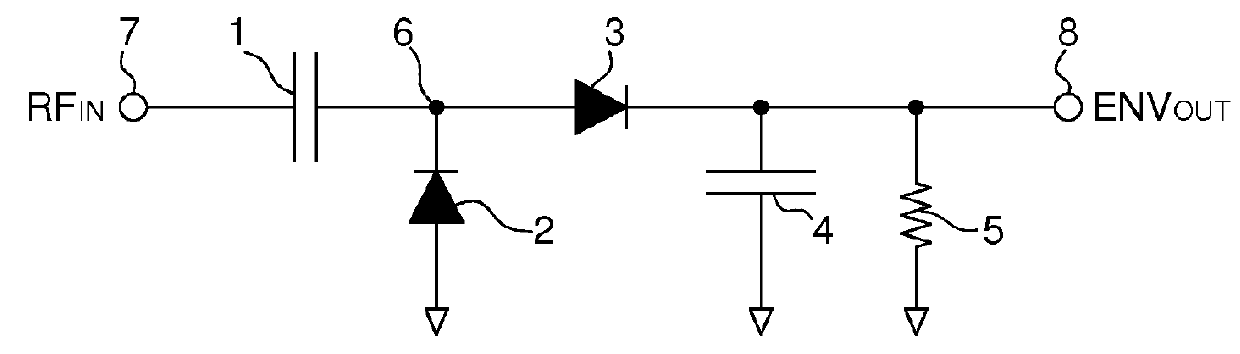
[0020]FIG. 1 shows an envelope detector circuit using a voltage doubler circuit, as known in the prior art. This envelope detector circuit comprises an input capacitor 1, connected in series with the input 7, to which can be applied an input signal RFIN. A pair of diodes 2 and 3 is arranged as a full-wave rectifier with respect to node 6 which is connected to input capacitor 1, and a second capacitor 4 is connected in parallel across the circuit output. The series capacitor 1 and the diode 2 together form a clamping circuit which builds a DC voltage across the series capacitor 1. If the diodes are taken as being ideal, then the DC voltage at output 8 will theoretically become equal to the peak-to-peak amplitude of the RF input voltage once capacitors 1 and 4 are charged. A resistor 5 provides a discharge path for capacitor 4, thereby ensuring that this capacitor does not remain fully charged, and that the envelope signal is presented at the output ENVOUT.

[0021]RFIN may for example b...


PUM


Abstract

An envelope detector circuit, suitable for use in RFID tags, includes a voltage doubler circuit and a biasing voltage generating circuit which comprises components matched respectively to rectifying components of the voltage doubler circuit. A rectifying component of this voltage doubler circuit is formed by a transistor controlled by the biasing voltage generating circuit which provides a biasing voltage to a control gate of this transistor, the biasing voltage generating circuit being arranged so as to permit a determined forward biasing current to flow through the transistor and further rectifying elements of the voltage doubler circuit. This embodiment provides fast, highly sensitive detection of envelope waveforms in input signals. Thanks to the matched rectifying components, efficiency variations due to variations in manufacturing process can be eliminated. The envelope detector circuit is further arranged for maintaining a stable detection independent of variations in temperature.

Description

[0001]This application claims priority from European Patent Application No. 13193326.9 filed 18 Nov. 2013, the entire disclosure of which is incorporated herein by reference.TECHNICAL FIELD[0002]The present invention relates to the field of envelope detector circuits and in particular, but not exclusively, to low-power circuits for detecting envelope waveforms in amplitude-modulated signals.BACKGROUND OF THE INVENTION[0003]Envelope detectors are commonly used for demodulating low-frequency information content from higher-frequency carrier signals. An example of such an application is in RFID chips, for example, where circuitry is required to extract amplitude modulation envelope information from received radio-frequency signals.[0004]In RFID chips, envelope detectors can be used to convert the amplitude modulated signal sent by a tag reader into a so-called baseband signal which contains the modulation signal, without the radio frequency carrier signal present in the reader signal. ...

Claims


Application Information

Patent Timeline
Patent Type & Authority Patents(United States)
IPC IPC(8): G06K19/06G06K7/00G01R19/04H03D1/10G06K19/07H03D1/18H04L27/06
CPCG01R19/04G06K7/0008G06K19/07G06K19/0713H03D1/10H03D1/18H04L27/06H03D2200/0011H03D2200/0043H03D2200/0098H04B5/0056
Inventor PILLIN, NICOLASSTOJANOVIC, GORANGHUELDRE, TONY
Owner EM MICROELECTRONIC-MARIN
Why Eureka
Try Eureka