Semiconductor optical devices

a technology of semiconductors and optical devices, applied in semiconductor lasers, fluorescence/phosphorescence, instruments, etc., can solve problems such as affecting current-voltage or impedance characteristics, and achieve the effect of simple and small construction

Inactive Publication Date: 2009-03-17
UNIV COLLEGE CARDIFF CONSULTANTS LTD
View PDF10 Cites 4 Cited by
  • Summary
  • Abstract
  • Description
  • Claims
  • Application Information

AI Technical Summary

Benefits of technology

[0005]We have now devised semiconductor optical devices which provide both light emission and light detection, for example enabling integration of an analytical system and providing a number of consequent advantages, but also of potential use in other applications: the devices may be of simple and small construction, enabling them to be used in the field.
[0019]Preferably a reverse bias applied to the photodetector places the diode close to its breakdown point: thus, in use, avalanche photo-detection occurs, thus substantially increasing the detection signal.
[0021]It will be appreciated that the above-described devices in accordance with the present invention may be miniaturised and mass produced, to provide mass-produced devices which are inexpensive yet reliable. Moreover, the samples may be positioned very closely to both the light emitter region and the light receiving region of the device, providing for high detection efficiency. It is particularly advantageous to provide for independent testing by means of an array of emitters / detectors on the same device.
[0023]This device is accordingly a single-channel device for use with a single sample (or a single sample at a time). The device may be constructed to a very small size and inexpensively, so that it can be used with ease in the field, and may indeed comprise a single use or disposable device.

Problems solved by technology

Instead, the device may be such that the received light affects an electrical property of the device and so alters its current-voltage or impedance characteristic.

Method used


Image

  • Semiconductor optical devices
  • Semiconductor optical devices
  • Semiconductor optical devices

Examples


Embodiment Construction

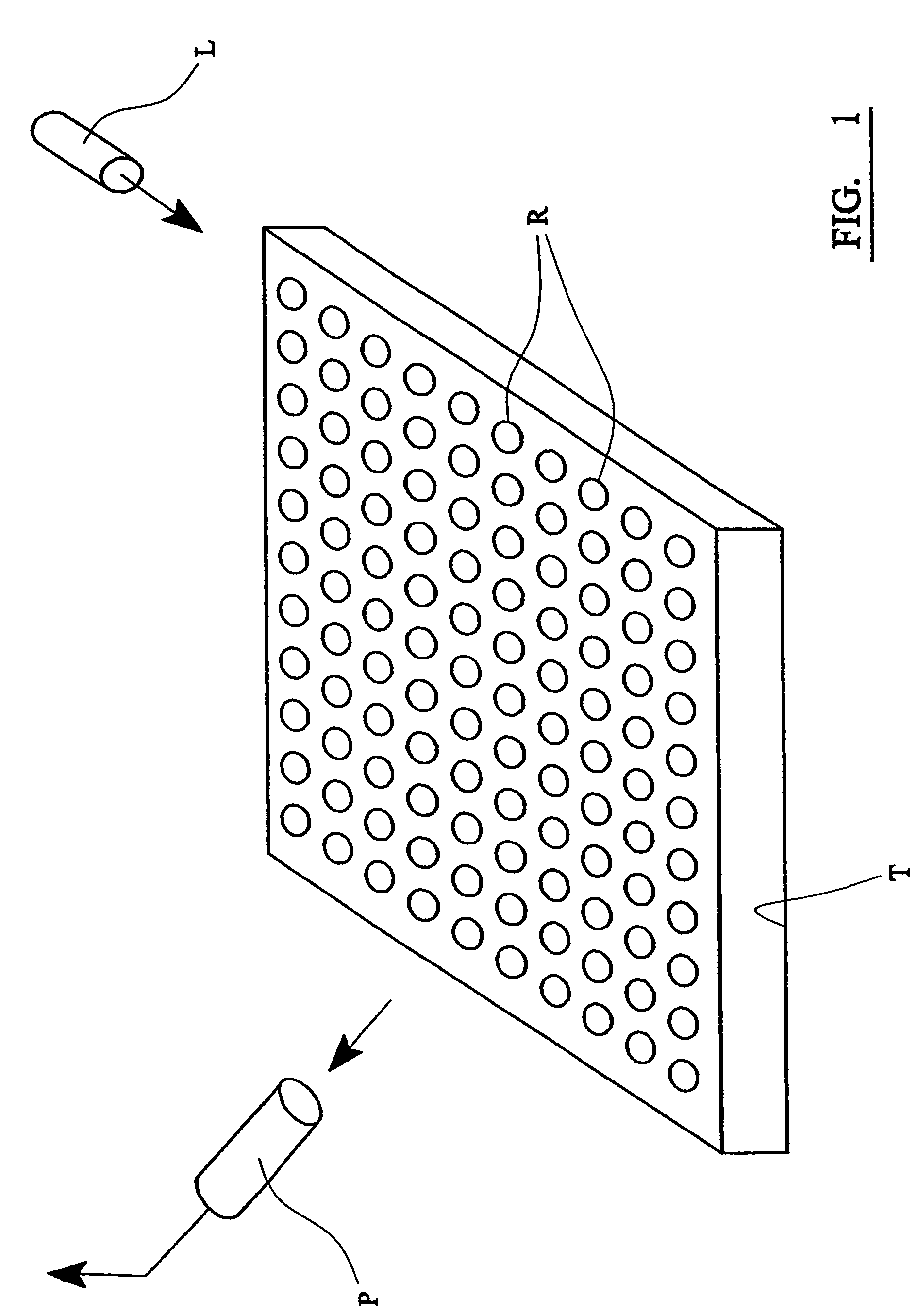
[0041]Referring to FIG. 1, there is shown a prior art system for the optical analysis of an array of biological samples, each of the samples being marked with a fluorescent dye. The system comprises a tray T the upper surface of which is formed with a two-dimensional array of recesses or wells R which receive respective samples. A laser or other source S is provided to direct light onto the samples: means are provided for scanning the light beam onto the samples in succession. A photodetector P is provided to pick up the light emitted, by fluorescence, from the successive samples, the output of the photodetector being passed to a processing unit.

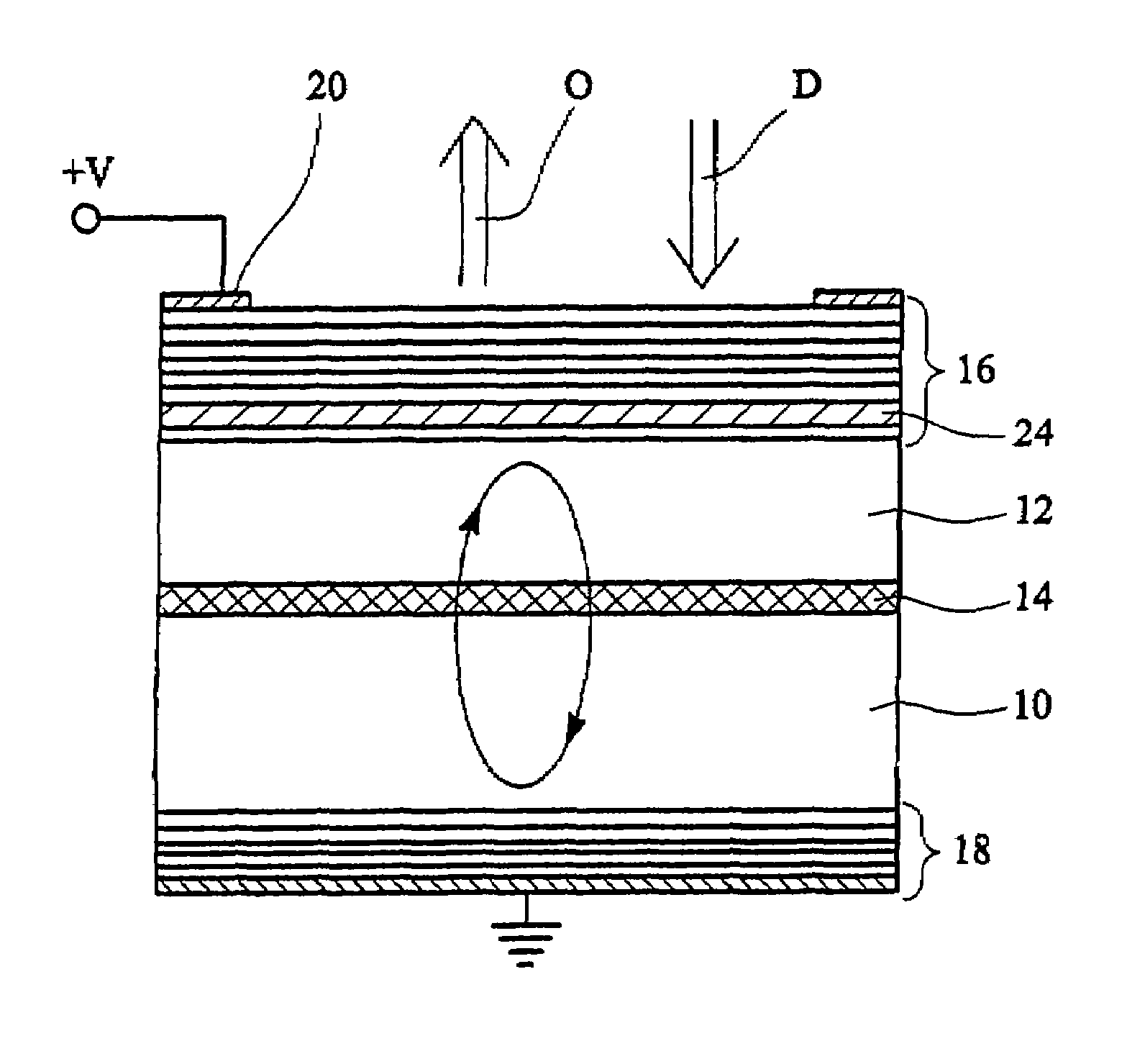
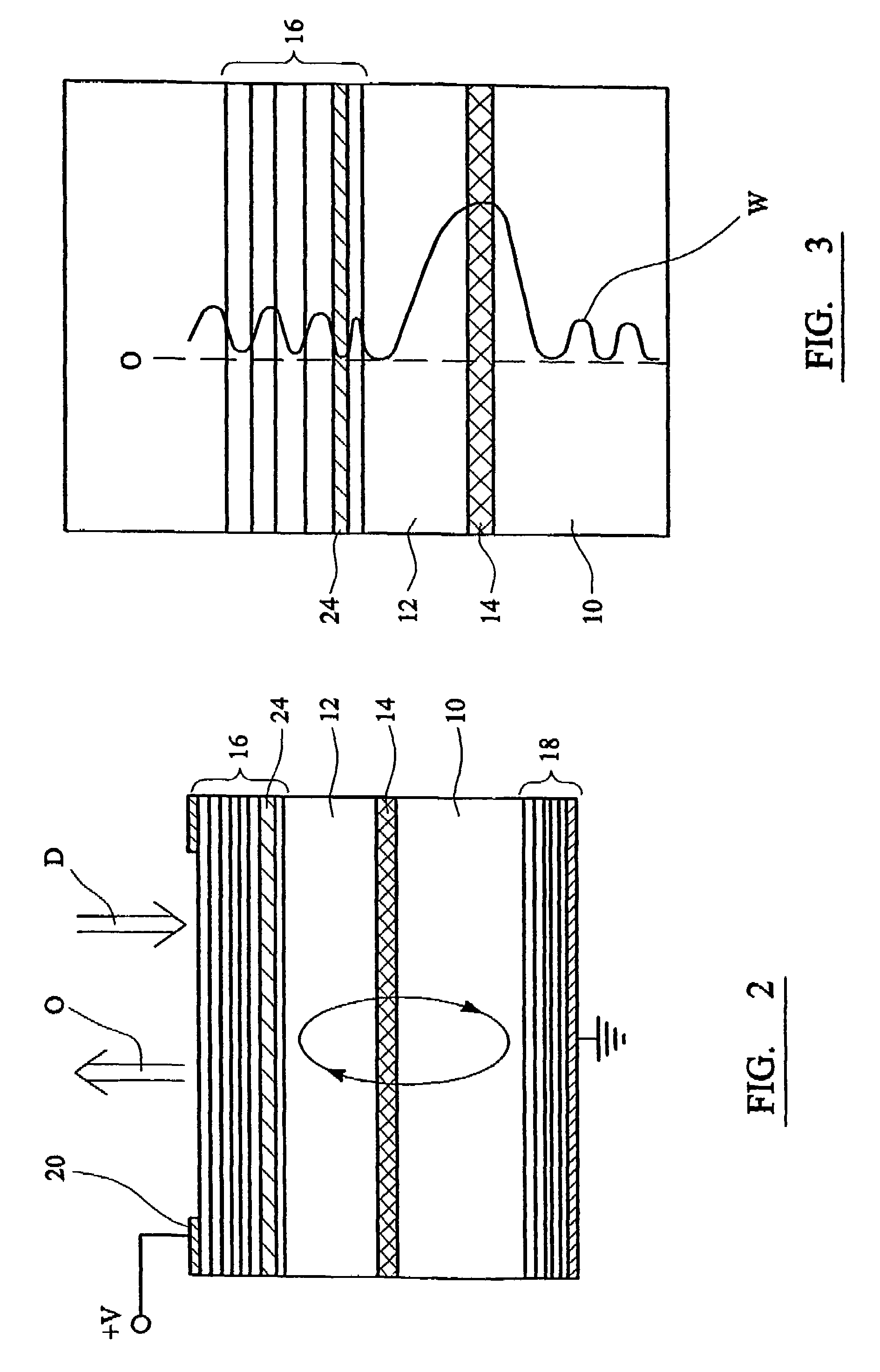
[0042]Referring to FIG. 2, there is shown a semiconductor device in accordance with the present invention in the form of a vertical-cavity, surface-emitting laser (or VCSEL), for use in performing an analytical test on a biological sample. The device comprises a semiconductor substrate having cavity layers 10,12 and an intermediate gain mate...


PUM

PropertyMeasurementUnit
refractive indexaaaaaaaaaa
wavelengthaaaaaaaaaa

Abstract

A semiconductor optical device (e.g. a resonant cavity device in this form of an LED or a laser) comprises a single substrate arranged for emitting light (O) for incidence on a sample or other element and also responsive to light (D), e.g. of a different wavelenght, received back from this sample or other element: the device further comprises means for monitoring a characteristic (e.g. its current-voltage characteristic) which varies in dependence upon the light (D) received back from the sample or other element.

Description

BACKGROUND OF THE INVENTION[0001]1. Field of the Invention[0002]The present invention relates to semiconductor optical devices, particularly but not solely for use in the field of bio-chemical or bio-medical analysis.[0003]2. State of the Art[0004]The use of optical techniques for the analysis of biological samples is a field of increasing importance, particularly in view of its potential for analysis at a molecular level. Various optical systems have been proposed hitherto: these systems have generally made use of a laser or other light emitter for directing light onto samples, typically successive samples in an array, and a separate photodetector for picking up light from the individual samples; typically the samples have been marked with a fluorescent dye, such that the incident light stimulates each sample to cause the emission of light of a different wavelength, which is picked up by the photodetector. Hitherto, such systems have been of large and complicated construction, for ...

Claims


Application Information

Patent Timeline
Patent Type & Authority Patents(United States)
IPC IPC(8): H01L27/15G01N21/64H01L31/0232H01L31/173H01S5/026H01S5/183H01S5/42
CPCH01L31/107H01L31/167H01S5/18388G01N2201/0612H01S5/0264H01S5/06808H01S5/141H01S5/2022H01S5/423
Inventor SUMMERS, HUW DAVID
Owner UNIV COLLEGE CARDIFF CONSULTANTS LTD
Why Eureka
Try Eureka