
ESD protection circuit and integrated circuit

a protection circuit and integrated circuit technology, applied in the direction of semiconductors, electrical devices, transistors, etc., can solve the problems of difficult to avoid damage to electronic elements or systems, etc., and achieve low parasitic capacitance, good esd protection capability, and performance reduction of the integrated circuit

Active Publication Date: 2016-06-28
NATIONAL TAIWAN NORMAL UNIVERSITY
View PDF5 Cites 1 Cited by
  • Summary
  • Abstract
  • Description
  • Claims
  • Application Information

AI Technical Summary

Benefits of technology

The invention provides an ESD protection circuit and an integrated circuit that have excellent ESD protection with low parasitic capacitance and do not negatively impact the performance of the integrated circuit. This is achieved through the use of a silicon-controlled rectifier element and an inductive element that work together to reduce parasitic capacitance and ensure good ESD protection.

Problems solved by technology

Electrostatic discharge (ESD) issue is a key factor to cause the damage to the most electronic elements or systems.
ESD is usually formed by the human cause and also difficult to be avoided.
Therefore, the electronic element or system will be damaged by the ESD.
This kind of damage may result in the permanent harm for the semiconductor device or computer system and the electronic product or system thus malfunctions.
However, for the scaled-down transistor, ESD is the main factor influencing the reliability thereof.
Especially in the application of the high-frequency integrated circuit, with the operation frequency from several GHz to dozens of GHz and even to hundreds of GHz for example, the ESD protection circuit not only needs a sufficiently high ESD immunity but also a very low parasitic capacitance, or the loading caused by the parasitic capacitance will result in the performance reduction of the circuit.

Method used


Image

  • ESD protection circuit and integrated circuit
  • ESD protection circuit and integrated circuit
  • ESD protection circuit and integrated circuit

Examples


Embodiment Construction

[0026]The present invention will be apparent from the following detailed description, which proceeds with reference to the accompanying drawings, wherein the same references relate to the same elements.

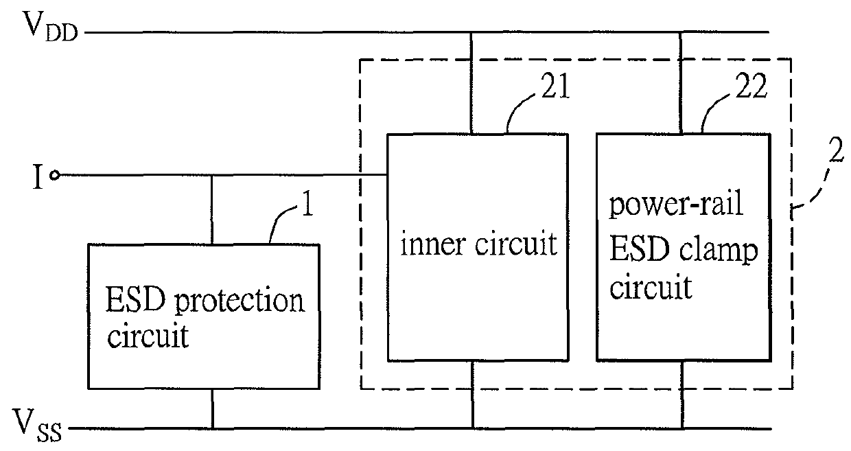
[0027]FIG. 1 is a schematic diagram of an ESD protection circuit 1 cooperated with a high-frequency circuit 2 according to a preferred embodiment of the invention.

[0028]As shown in FIG. 1, the high-frequency circuit 2 is electrically coupled to a first voltage VDD and a second voltage VSS, and the ESD protection circuit 1 acts as the ESD protection circuit of the high-frequency circuit 2. The first voltage VDD can be a positive voltage and the second voltage VSS can be zero (i.e. grounded), for example, and the voltage difference between the first voltage VDD and the second voltage VSS is the operation frequency of the high-frequency circuit 2. The high-frequency circuit 2 has at least a signal input end I or at least a signal output end, and the ESD protection circuit 1 is electrical...


PUM


Abstract

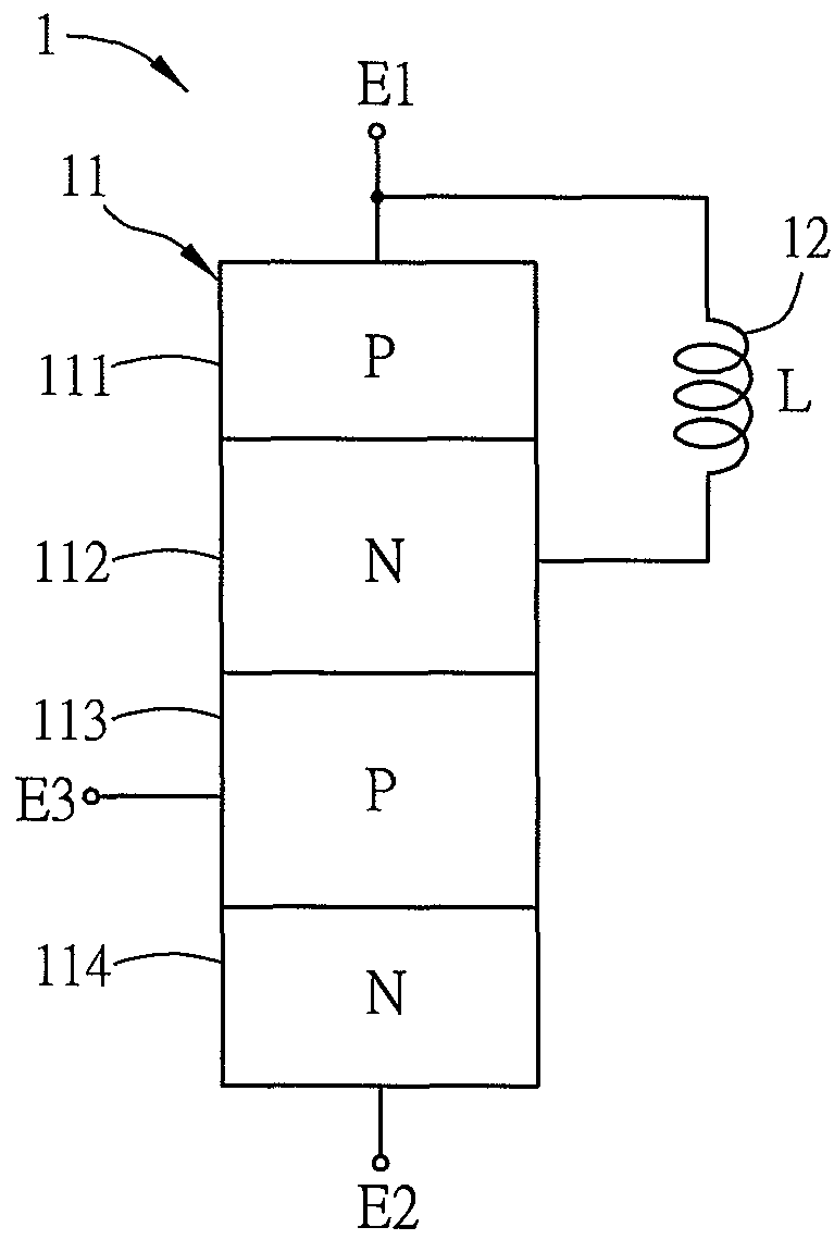
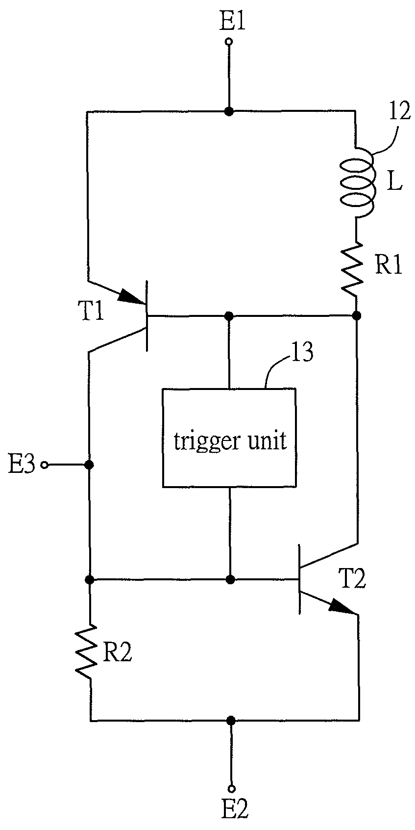
An ESD protection circuit is cooperated with a high-frequency circuit and includes a silicon-controlled rectifier element and an inductive element. The silicon-controlled rectifier element is formed by the sequential connection of a first P-type semiconductor material, a first N-type semiconductor material, a second P-type semiconductor material and a second N-type semiconductor material. The silicon-controlled rectifier element has a first end and a second end, and the first end is electrically coupled with the first P-type semiconductor material while the second end is electrically coupled with the second N-type semiconductor material. One end of the inductive element is electrically coupled with the first end and the other end thereof is electrically coupled with the first N-type semiconductor material, or one end of the inductive element is electrically coupled with the second end and the other end thereof is electrically coupled with the second P-type semiconductor material.

Description

CROSS REFERENCE TO RELATED APPLICATIONS[0001]This Non-provisional application claims priority under 35 U.S.C. §119(a) on Patent Application No(s). 103116734 filed in Taiwan, Republic of China on May 12, 2014, the entire contents of which are hereby incorporated by reference.BACKGROUND OF THE INVENTION[0002]1. Field of Invention[0003]The invention relates to an electrostatic discharge (ESD) protection circuit and an integrated circuit.[0004]2. Related Art[0005]Electrostatic discharge (ESD) issue is a key factor to cause the damage to the most electronic elements or systems. ESD is usually formed by the human cause and also difficult to be avoided. For example, the static electricity will be accumulated in the human body, appliances, storage devices and even electronic elements in the manufacturing, production, assembly, testing, storage and conveying process of the electronic element or system. The workers may unknowingly make these objects contact each other and an ESD path is thus ...

Claims


Application Information

Patent Timeline
Patent Type & Authority Patents(United States)
IPC IPC(8): H01L27/02
CPCH01L27/0262H01L27/0248
Inventor LIN, CHUN-YU
Owner NATIONAL TAIWAN NORMAL UNIVERSITY
Learn More