Reconfigurable electronic devices and operation method thereof

a technology of electronic devices and operating methods, applied in semiconductor devices, instruments, electrical devices, etc., can solve the problems of large reduction of the degree of freedom of wire lines, increased parasitic resistance or capacitance components, and increased voltage coupling with other wire lines, so as to improve the degree of integration, the degree of freedom of driving of the device, and the effect of diversity of functions

Active Publication Date: 2016-07-26
SEOUL NAT UNIV R&DB FOUND
View PDF4 Cites 7 Cited by
  • Summary
  • Abstract
  • Description
  • Claims
  • Application Information

AI Technical Summary

Benefits of technology

[0018]First, in the reconfigurable electronic device of the related art, in the implementation of the device using the junction between the Si nanowire and the Ni silicide, there is an essential problem in accurate control of the position of the junction, and in the implementation of the two top-gates, the two top-gates are not self-aligned with the junction, so that the parasitic resistance or the capacitance component is greatly increased. In order to solve the problem, in the present invention, gate electrodes are located in a lower portion so as to freely adjust the resistance of Schottky junction of the device; and in order to accurately control the positions of the gate electrodes, the source and drain electrodes, and the channel in the device, photolithography process is used, so that reproducibility of position control and adjustability of position are to be improved.
[0059]Due to such an advantage, in the reconfigurable electronic device according to the present invention, the above-described localized electrical doping can be performed. As a result, the change of the type (p-n dioden-p diode, n-type FETp-type FET) of the device, the modulation of the channel length, the implementation of various multi-functional devices such as diode logics can be performed. In addition, in the reconfigurable electronic device according to the present invention, in the implementation of the reconfigurable circuit, diversity of the function, the degree of freedom of driving of the device, and the degree of integration can be improved.

Problems solved by technology

First, in the reconfigurable electronic device of the related art, in the implementation of the device using the junction between the Si nanowire and the Ni silicide, there is an essential problem in accurate control of the position of the junction, and in the implementation of the two top-gates, the two top-gates are not self-aligned with the junction, so that the parasitic resistance or the capacitance component is greatly increased.
Second, in the reconfigurable electronic device of the related art, in the changing of the type of the device (for example, nMOSFET→pMOSFET), a voltage is always applied to one of the two top-gates, and thus, voltage coupling with other wire lines and leakage current may occur, so that the degree of freedom of the wire lines is greatly decreased.
In order to solve the problem, in the reconfigurable electronic device of the related art, although the non-volatile memory function can be applied to the gate insulating film, the Eot is increased, so that current driving performance is greatly deteriorated, and it is difficult to achieve miniaturization down to an infinitesimal channel length range (L<10 nm).
Third, in the reconfigurable electronic device of the related art, even in the case where the device is operated as any type of the MOSFETs, one of the source and the drain necessarily has a Schottky junction, and thus, if a reverse bias is applied to the Schottky junction, large low-frequency noise occurring in the Schottky junction essentially limits applications of the device.

Method used


Image

  • Reconfigurable electronic devices and operation method thereof
  • Reconfigurable electronic devices and operation method thereof
  • Reconfigurable electronic devices and operation method thereof

Examples


first embodiment

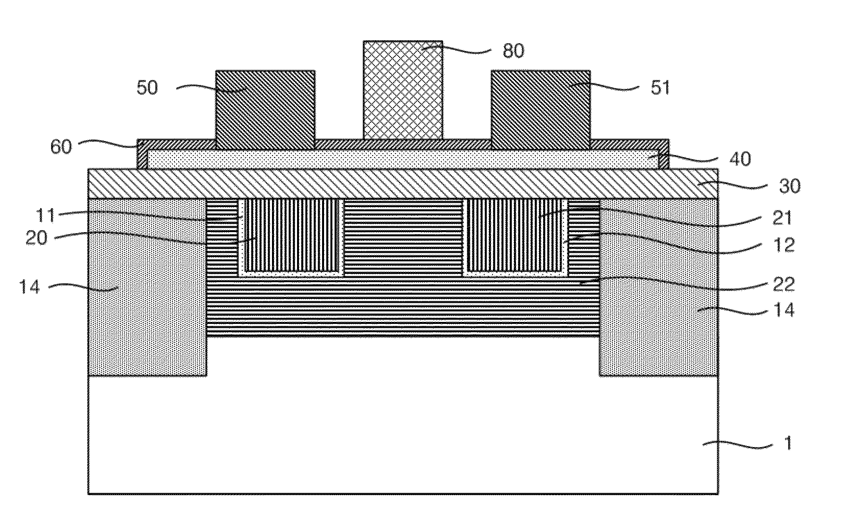
[0071]A configuration of a reconfigurable electronic device according to the first embodiment of the present invention will be described in detail. FIG. 1 is a cross-sectional diagram illustrating the reconfigurable electronic device according to the first embodiment of the present invention.

[0072]In FIG. 1, the reconfigurable electronic device according to the embodiment is a reconfigurable electronic device on the basis of a lower electrode having a non-volatile memory function and is configured to include: a substrate 1; a plurality of lower electrodes 20, 21, and 22 which are formed on the substrate to be electrically isolated from each other; inter-electrode insulating films 11 and 12; an isolation insulating film 14 for electrical isolation from adjacent different devices; a lower gate insulating film 3 formed on the lower electrodes; a body 40 formed on the lower gate insulating film; a first upper electrode 50 formed in a first region on the body; a second upper electrode 51...

second embodiment

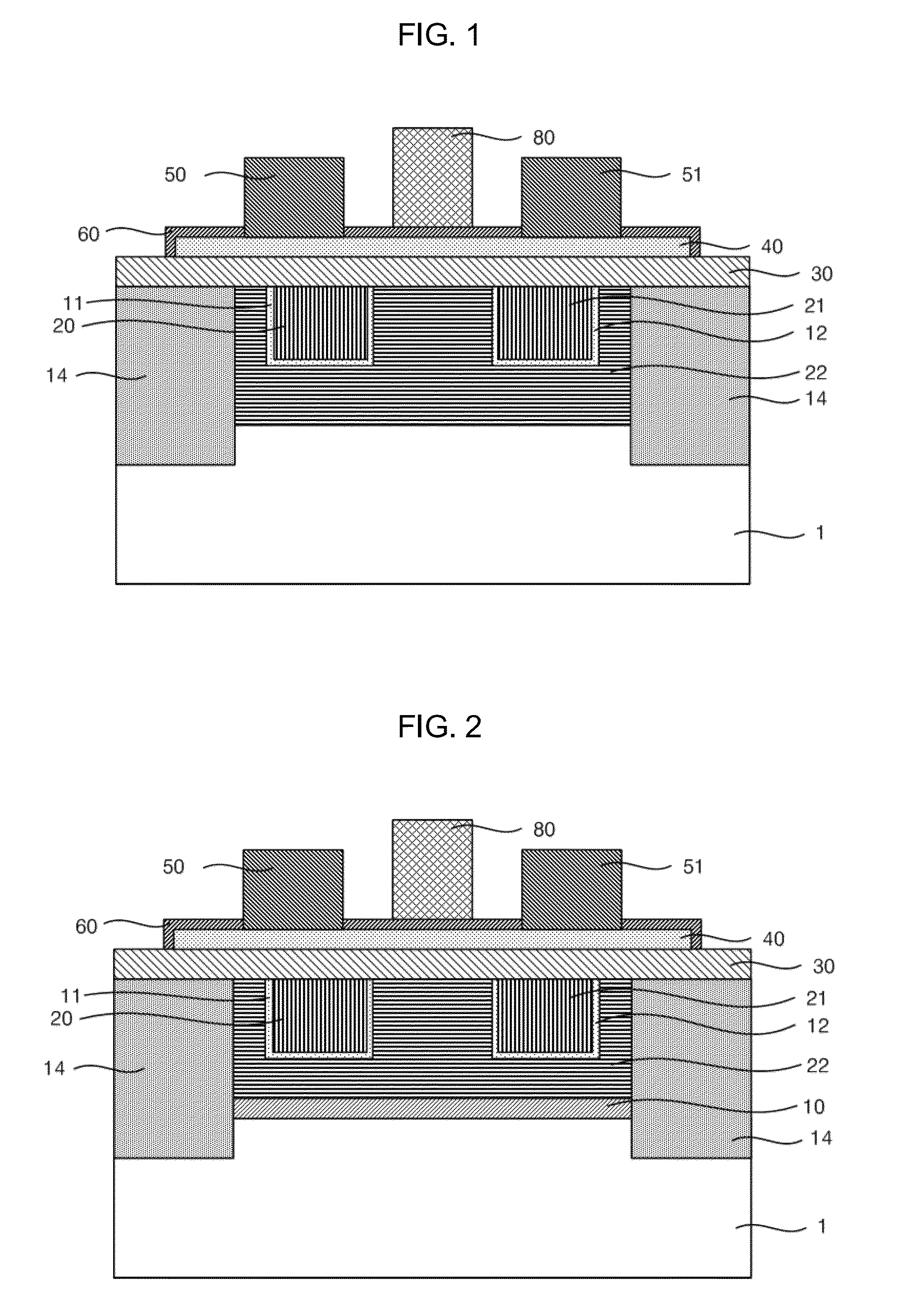
[0087]A reconfigurable electronic device according to a second embodiment of the present invention is configured to further include an insulating film 10 between the lower electrode and the substrate in the electronic device according to the first embodiment, so that the lower electrodes and the substrate are electrically isolated.

[0088]FIG. 2 is a cross-sectional diagram illustrating the reconfigurable electronic device according to the second embodiment of the present invention.

[0089]Referring to FIG. 2, in the case where the substrate is configured with a semiconductor material or a conductive material, preferably, the electronic device further includes the insulating film 10 between the substrate and the lower electrodes, so that the lower electrodes are electrically isolated from the substrate.

[0090]In particular, preferably, the entire bottom surface of the lower electrode surrounding the other lower electrodes is in contact with the insulating film 10.

[0091]Due to the configu...

third embodiment

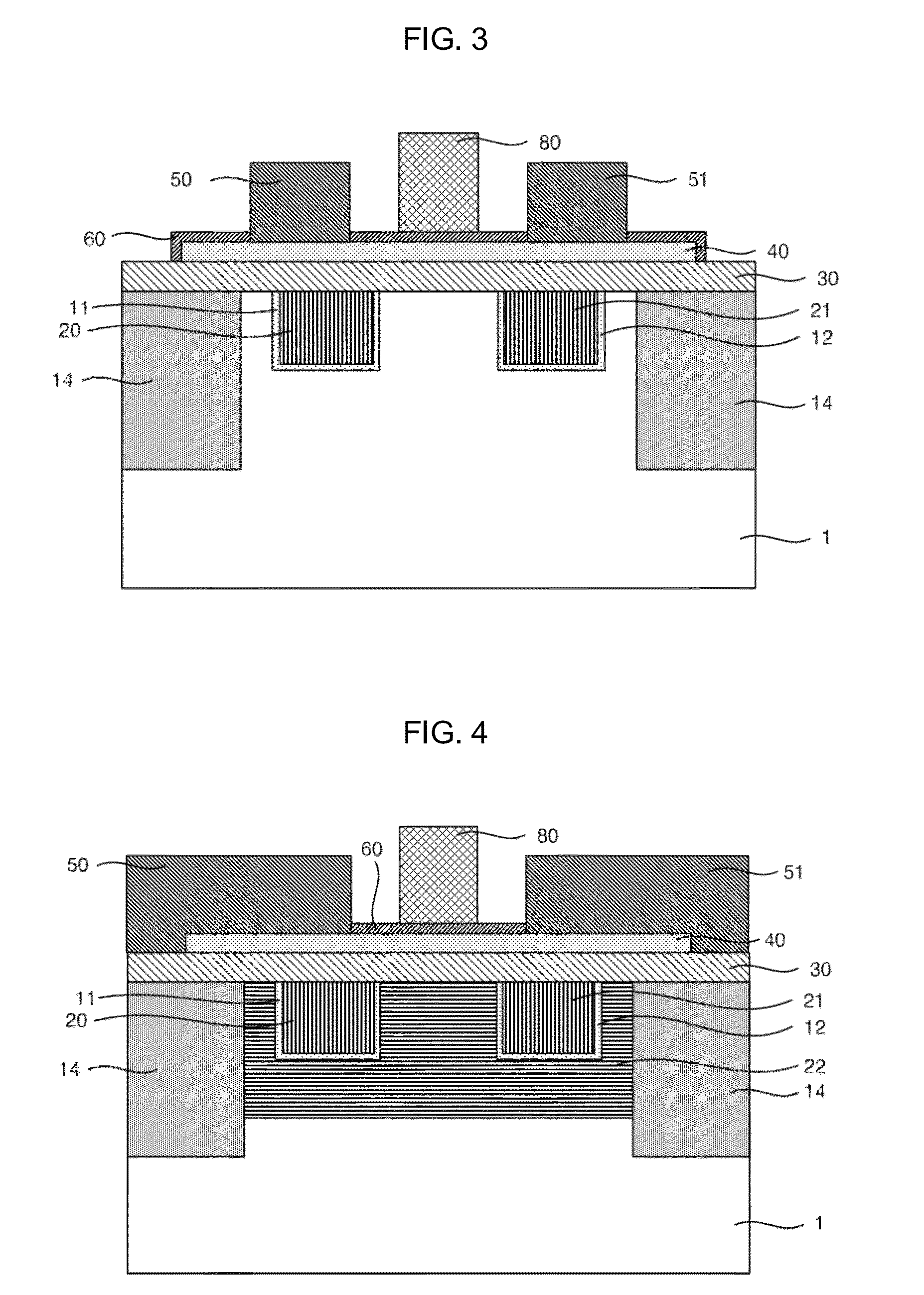
[0093]A reconfigurable electronic device according to a third embodiment of the present invention is configured so that the substrate of the electronic device according to the first embodiment is operated as a lower electrode.

[0094]FIG. 3 is a cross-sectional diagram illustrating the reconfigurable electronic device according to the third embodiment of the present invention. Referring to FIG. 3, the reconfigurable electronic device according to the embodiment is configured to include a substrate 1; one or two or more lower electrodes 20 and 21 which are formed on the substrate and are electrically isolated from the substrate; a lower gate insulating film 30 which is formed on a portion of the substrate and the lower electrodes; a body 40 which is formed on the lower gate insulating film; a first upper electrode 50 which is formed on a first region of the body; a second upper electrode 51 which is formed on a second region of the body and is separated from the first upper electrode b...


PUM


Abstract

Provided is a reconfigurable electronic device which is implemented by forming independent upper gates and lower gates, wherein in comparison with an existing reconfigurable electronic device having the same function, a degree of integration is greatly increased, a non-volatile memory function is included in the device, and in operation of a reconfigurable circuit based on an independent lower electrode array, dynamic parasitic component is decreased and a complexity of wire lines can be reduced, so that power consumption can be reduced. In addition, in comparison with an existing reconfigurable electronic device, the device exhibits remarkably excellent performance in terms of various characteristics such as diversity of functions of a multi-functional device, alignment margin in process, performance of implementation of infinitesimal electrical doping in a channel, compatibility with bottom-up and top-down method in process, and compatibility with a 1D or 2D material.

Description

FUNDING STATEMENT[0001]This invention was supported by Samsung Research Funding Center of Samsung Electronics under Project Number SRFC-IT1301-08.CROSS-REFERENCE TO RELATED PATENT APPLICATION[0002]This application claims the benefit of Korean Patent Application No. 10-2014-0109727, filed on Aug. 22, 2014, in the Korean Intellectual Property Office, the disclosure of which is incorporated herein in its entirety by reference.BACKGROUND OF THE INVENTION[0003]1. Field of the Invention[0004]The present invention relates to a reconfigurable electronic device and, more particularly, to a reconfigurable electronic device having a non-volatile memory function which can be reconstructed by implementing independent lower electrodes including the non-volatile memory function and electrically adjusting a body of a 1D or 2D material or a thin semiconductor thin film.[0005]2. Description of the Prior Art[0006]Si-based sub-8 nm 3D (three-dimensional) devices are expected to be used in 2020s. Due to...

Claims


Application Information

Patent Timeline
Patent Type & Authority Patents(United States)
IPC IPC(8): G11C16/12G11C16/04G11C16/14H01L29/423H01L29/78H01L29/792
CPCG11C16/0466H01L29/42344H01L29/42348H01L29/42352H01L29/7881H01L29/792H01L29/78391H01L29/4234G11C16/14H10B41/30G11C16/12
Inventor LEE, JONG-HO
Owner SEOUL NAT UNIV R&DB FOUND
Why Eureka
Try Eureka