Semiconductor device

a technology of semiconductor devices and semiconductor chips, applied in semiconductor devices, semiconductor/solid-state device details, electrical apparatus, etc., can solve problems such as difficult to improve the module yield rate, connection failure, and connection failure, and achieve the effect of improving the mounting quality of each semiconductor chip

Active Publication Date: 2016-08-16
FUJI ELECTRIC CO LTD
View PDF17 Cites 2 Cited by
  • Summary
  • Abstract
  • Description
  • Claims
  • Application Information

AI Technical Summary

Benefits of technology

[0014]Furthermore, a wide bandgap (WBG) device typified by an SiC semiconductor or the like, the application of which is increasing recently, is such that, taking into account the yield rate due to wafer defects, it is necessary to increase volume by attempting multichip mounting of a small semiconductor chip of in the region of 2 mm to 5 mm square. The small semiconductor chip is such that positioning between a DCB substrate and the semiconductor chip, and of the semiconductor chip and a printed substrate having conductive posts, is difficult compared with when using the existing Si, and joining of a predetermined electrode pad and a conductive post is difficult, on top of which, as parallel connection is carried out using a large number of semiconductor chips, there is an unresolved problem in that it is predicted that it will be difficult to improve the module yield rate when the heretofore described kind of semiconductor chip connection failure occurs. Therefore, embodiments of the invention provide a semiconductor device that may improve the mounting quality of each semiconductor chip.
[0016]According to embodiments of the invention, when having a first conductive post and a plurality of second conductive posts individually joined by a joining material to a first electrode pad and second electrode pad included on one surface of a semiconductor chip, the second conductive posts on the side near the first conductive post are arrayed avoiding a short-circuit prevention region at a distance such that the joining material of the first conductive post and the joining material of the second conductive posts do not link, because of which it is possible to reliably prevent the first conductive post and the second conductive posts on the side near the first conductive post from being short-circuited by the joining material. Consequently, it is possible to improve the mounting quality of each semiconductor chip.

Problems solved by technology

However, the existing examples described in the publications noted above are such that, focusing on semiconductor chip temperature rise, conductive posts are simply joined to an electrode on one surface of a semiconductor chip, and absolutely no consideration is given to a short-circuit caused by solder between electrode pads when two or more electrode pads are disposed on one surface of a semiconductor chip.
Because of this, it may happen that connection failure occurs due to a short-circuit between the emitter electrode pad 205a and gate electrode pad 205b.
Also, when using a solid phase diffusion joining material such as metal particles typified by nano-Ag or the like, it may happen that the joining material spreads in the horizontal plane due to a process such as pressurization when joining, because of which, in the same way as with the solder, there is an unresolved problem in that it may happen that the joining material on individual electrode pads of the semiconductor chip comes into contact, and connection failure due to a short-circuit occurs.
The small semiconductor chip is such that positioning between a DCB substrate and the semiconductor chip, and of the semiconductor chip and a printed substrate having conductive posts, is difficult compared with when using the existing Si, and joining of a predetermined electrode pad and a conductive post is difficult, on top of which, as parallel connection is carried out using a large number of semiconductor chips, there is an unresolved problem in that it is predicted that it will be difficult to improve the module yield rate when the heretofore described kind of semiconductor chip connection failure occurs.

Method used


Image

  • Semiconductor device
  • Semiconductor device
  • Semiconductor device

Examples


first embodiment

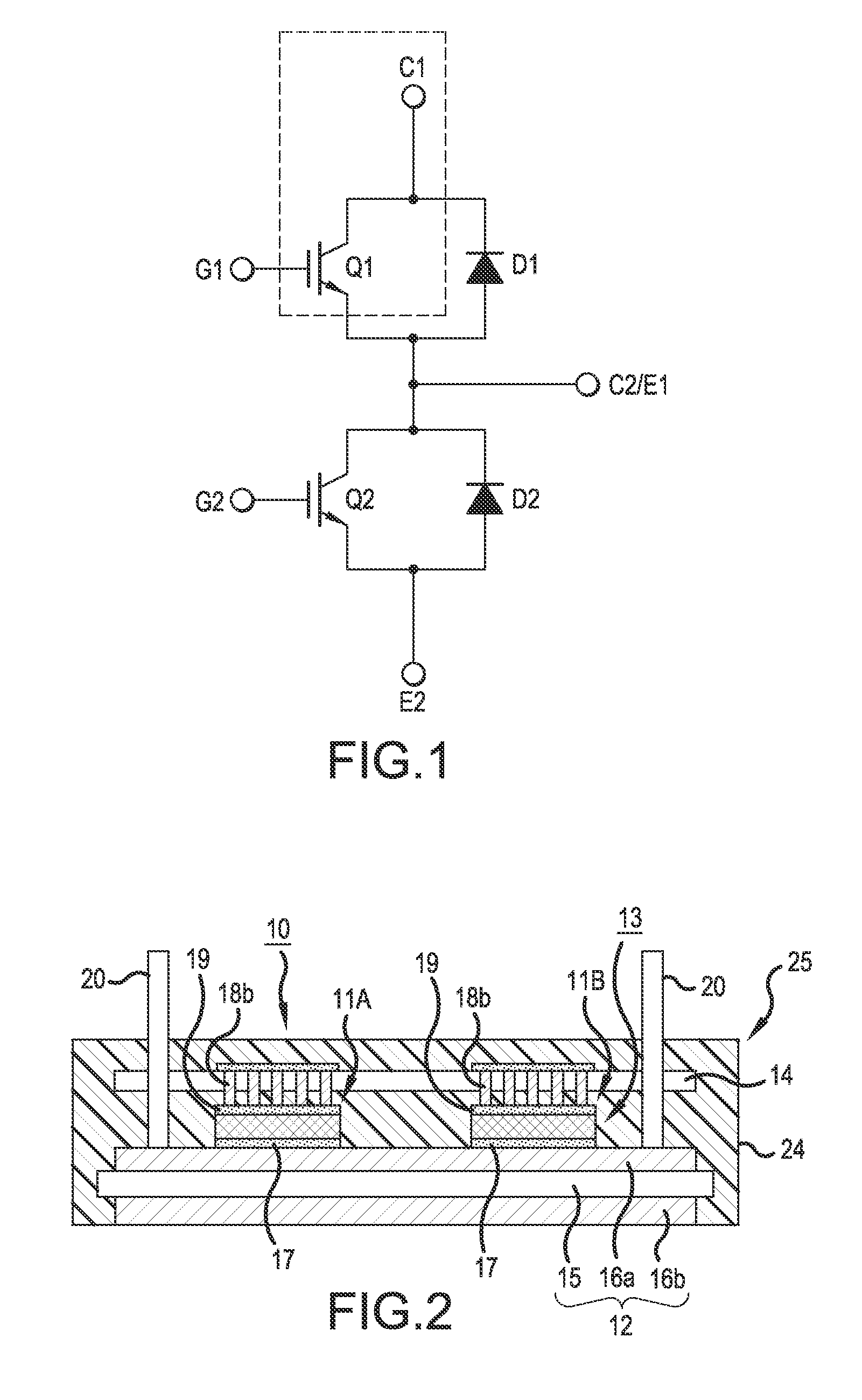
[0032]FIG. 2 is a sectional view showing the invention. A transistor for a power semiconductor device with a large rated current is such that a process whereby semiconductor chips with a small rated current are used in parallel, thus increasing the rated current of the whole, is carried out. FIG. 2 shows the portion of the first transistor Q1 and first collector terminal C1 shown by the broken lines in FIG. 1 as two semiconductor elements 11A and 11B and two pin-form conductors 20 formed in parallel. An insulating substrate 12 is configured of a ceramic substrate 15 of alumina, or the like, with good heat conductivity, and copper plates 16a and 16b individually attached to the front and back surfaces of the ceramic substrate 15. A predetermined semiconductor circuit 13 for connecting a plurality of power devices disposed on the copper plate 16a is formed on the copper plate 16a on the front surface side of the insulating substrate 12. Although not shown in FIG. 2, a control electrod...

fourth embodiment

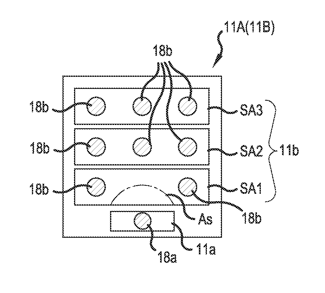
[0050]However, in the fourth embodiment, an equal number of the second conductive posts 18b are disposed at equal intervals in the intermediate sub-region SA2 and outer sub-region SA3, because of which there is no region in the intermediate sub-region SA2 or outer sub-region SA3 in which the value of the resistance caused by the second conductive posts 18b becomes excessive, and it is thus possible to suppress the amount of heat generated. Consequently, it is possible to reduce thermal stress, suppressing connection portion failures (joining material cracks, detachment, semiconductor chip cracks occurring due to solder tensile stress, short-circuits, and the like) caused by differences between the linear expansion coefficients of the second conductive posts 18b and the joining material, such as solder, and semiconductor chips 11A and 11B, and thus increasing reliability.

[0051]Next, a description will be given, accompanying FIG. 9, of a fifth embodiment of the invention. The fifth em...


PUM


Abstract

A semiconductor device including a semiconductor chip, a first electrode pad and second electrode pad included on one surface of the semiconductor chip, a first conductive post joined by a joining material to the first electrode pad, a plurality of second conductive posts joined by a joining material to the second electrode pad, and a printed substrate, disposed opposing the one surface of the semiconductor chip, on which is formed an electrical circuit to which the first conductive post and second conductive posts are connected. The second conductive posts on the side near the first conductive post are arrayed avoiding a short-circuit prevention region at a distance such that the joining material of the first conductive post and the joining material of the second conductive posts do not link.

Description

CROSS-REFERENCE TO RELATED APPLICATIONS[0001]This application is a continuation of International Application No. PCT / JP2014 / 000371, filed on Jan. 24, 2014, and is based on and claims priority to Japanese Patent Application No. JP 2013-012261, filed on Jan. 25, 2013. The disclosure of the Japanese priority application and the PCT application in their entirety, including the drawings, claims, and the specification thereof, are incorporated herein by reference.BACKGROUND[0002]1. Field[0003]Embodiments of the present invention relate to a semiconductor device wherein an electrode of a semiconductor chip mounted on an insulating substrate inside a semiconductor device is electrically connected via a conductive post to a printed substrate sealed inside the semiconductor device.[0004]2. Discussion of the Background[0005]A semiconductor device in which is mounted a power semiconductor element such as an IGBT (Insulated Gate Bipolar Transistor) or power-FET (Field Effect Transistor) is used ...

Claims


Application Information

Patent Timeline
Patent Type & Authority Patents(United States)
IPC IPC(8): H01L23/48H01L29/40H01L25/07H01L23/498H01L25/18
CPCH01L25/072H01L23/481H01L23/49811H01L23/49844H01L29/408H01L2224/92242H01L25/18H01L2224/0401H01L2224/06051H01L2224/06181H01L2224/11318H01L2224/13111H01L2224/16235H01L2224/16238H01L2224/291H01L2224/32225H01L2224/73253H01L2224/81815H01L2924/10253H01L2924/10272H01L2924/1203H01L2924/13055H01L2924/13091H01L2924/014H01L2924/01047H01L2924/01029H01L2924/01051H01L2924/01083H01L2924/1305H01L2924/00H01L23/053H01L23/3121H01L2224/29101H01L24/01H01L2224/0603H01L2924/00014H01L23/00H01L24/00
Inventor NAKAMURA, YOKONASHIDA, NORIHIRO
Owner FUJI ELECTRIC CO LTD
Why Eureka
Try Eureka