Tunnel junction fabrication

a technology of tunnel junctions and fabrication lines, applied in the direction of instruments, superconductor devices, heat measurement, etc., can solve the problems of limiting device performance and affecting junction quality, and achieve the effects of eliminating, or high quality

Active Publication Date: 2016-08-23
RGT UNIV OF CALIFORNIA
View PDF15 Cites 9 Cited by
  • Summary
  • Abstract
  • Description
  • Claims
  • Application Information

AI Technical Summary

Benefits of technology

[0007]The disclosed methods and apparatus enables fabrication of high quality, large area tunnel junction barriers for NIS or SIS tunnel junctions. For example, ALD and an aluminum wetting layer allow the formation of a nanometer scale insulating barrier on gold films. Electronic transport measurements confirm that single-particle electron tunneling is the dominant transport mechanism, and measured current-voltage curves demonstrate the viability of using these devices as self-calibrated, low temperature thermometers with a wide range of tunable parameters. The disclosed methods and apparatus enable superconducting technologies that involve deposited tunnel junction barriers and allows fabrication of high performance junction refrigerators.
[0008]Particular embodiments of the subject matter described in this specification can be implemented to realize one or more of the following advantages. Superconducting tunnel junction fabrication can be improved so as to eliminate, or at least significantly reduce, point defects in tunnel barriers that are fabricated using traditional approaches. These traditional defects can result in decoherence in SIS junctions that limit the performance of qubits and subgap leakage in NIS junctions that limits their cooling power. Point defects can also place an upper limit on the size and yield of superconducting tunnel junctions. For a fixed specific resistance (i.e., resistivity), the cooling power of an NIS junction refrigerator scales directly with junction area, thus the ability to fabricate larger junctions can vastly improve refrigeration capabilities.
[0009]Epitaxial deposition using ALD can rid the barrier of defects that prevent commercial viability. Further, ALD allows barrier thickness to be precisely tuned down to 0.02 nm, allowing for further improvements in device properties. Utilizing ALD, high quality tunnel barriers can now be deposited on materials that are non-oxidizing (i.e., do not natively oxidize), such as Au, or metals that form incomplete or conductive oxide layers, such as Cu and Ag.

Problems solved by technology

However, the diffusive nature of the thermal oxidation process leads to point defects in the tunnel barrier that affect junction quality.
Currently, barriers for tunnel junctions are created using diffuse oxidation processes that can limit device performance.

Method used


Image

  • Tunnel junction fabrication
  • Tunnel junction fabrication
  • Tunnel junction fabrication

Examples


Embodiment Construction

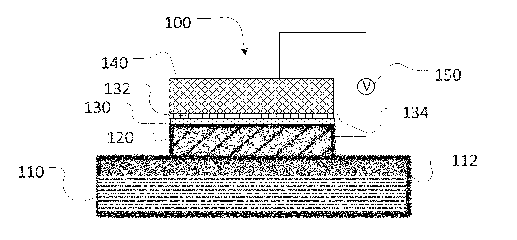
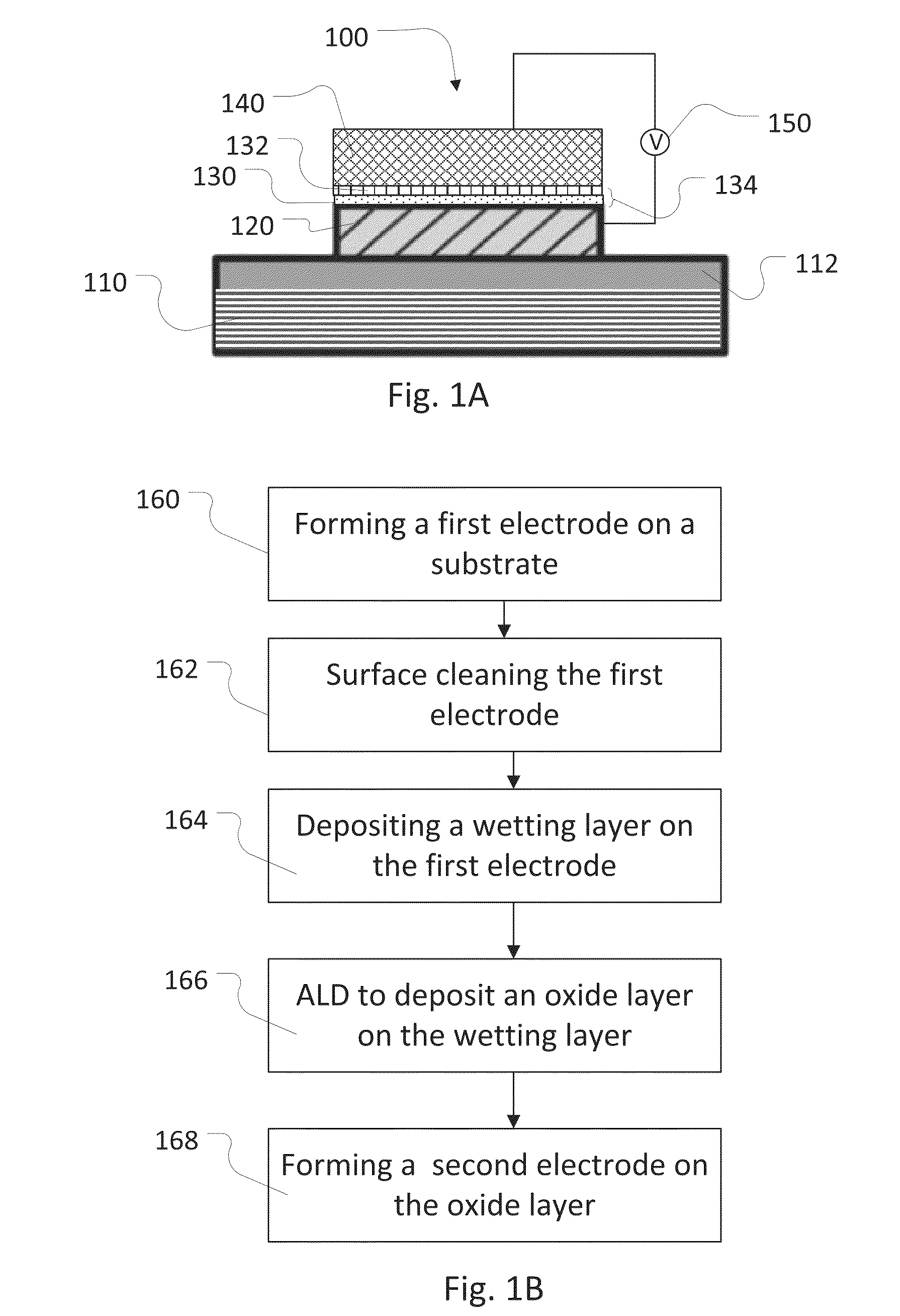
[0022]FIG. 1A shows a schematic of a normal-insulating-superconducting (NIS) junction 100. A substrate 110 supports a first electrode 120 that is deposited on the substrate. A wetting layer 130 is deposited on the first electrode 120, and an oxide layer 132 is deposited on the wetting layer 130. The wetting layer 130 and the oxide layer 132 together form a tunnel junction barrier 134. A second electrode 140 is deposited on the tunnel junction barrier 134. The first electrode 120 is formed of a normal (i.e., non-superconducting) material, for example, gold (Au). The second electrode 140 is formed of a superconducting material, for example, aluminum (Al). In other words, the NIS junction 100 is formed by the three components: the first electrode 120, which is a normal conductive metal layer, the tunnel junction barrier 134, which separates the first electrode 120 from the second electrode 140, and the second electrode 140, which is a superconducting metal layer. The substrate 110 can ...


PUM

PropertyMeasurementUnit
thicknessaaaaaaaaaa
areaaaaaaaaaaa
thicknessaaaaaaaaaa

Abstract

A method for fabricating a tunnel junction includes depositing a first electrode on a substrate, depositing a wetting layer having a thickness of less than 2 nm on the first electrode, using atomic layer deposition (ALD) to deposit an oxide layer on the wetting layer, and depositing a second electrode on the oxide layer. The wetting layer and the oxide layer form a tunnel barrier, and the second electrode includes a superconductor.

Description

CROSS-REFERENCE TO RELATED APPLICATION[0001]This application claimed priority to U.S. application Ser. No. 61 / 814,029 filed on Apr. 19, 2013, which is incorporated herein by reference.BACKGROUND[0002]This specification relates to tunnel junction fabrication, for example, superconducting junction fabrication. In recent years, superconducting tunnel junctions have become a viable technology for a wide range of cryogenic applications. There is intense interest in solid-state quantum computing based on a range of systems that include superconducting-insulating-superconducting (SIS) trilayers as the building blocks for quantum bits (qubits) in quantum computers. Normal-insulating-superconducting (NIS) junctions have been used as on-chip solid-state refrigerators and more recently as bulk cryogenic coolers.[0003]Both SIS and NIS technologies utilize pristine dielectric barriers a few nanometers thick to serve as tunnel junctions. These barriers are typically fabricated via thermal oxidati...

Claims


Application Information

Patent Timeline
Patent Type & Authority Patents(United States)
IPC IPC(8): H01L21/00H01L39/24H01L39/22G06N99/00G01K7/01
CPCH01L39/2493H01L39/223G06N99/002G01K7/01H01L39/22H01L39/228G06N10/00H10N60/10H10N60/12H10N60/0912H10N60/128
Inventor MOYERMAN, STEPHANIEKEATING, BRIAN
Owner RGT UNIV OF CALIFORNIA
Why Eureka
Try Eureka