
Integrated capacitor and method for producing the same

a technology of integrated capacitors and capacitors, which is applied in the manufacture of solid-state devices, semiconductor/solid-state devices, electric devices, etc., can solve the problems of spurious affecting the electric characteristics of the integrated circuit, the operating voltage of such integrated capacitors for high-voltage applications is limited, and the mechanical tension of monolithically integrated 3d capacitors with trench or hole structures for high operating voltages in the range of 600 v and above may be too high, so as to reduce the structural siz

Active Publication Date: 2016-09-27
FRAUNHOFER GESELLSCHAFT ZUR FOERDERUNG DER ANGEWANDTEN FORSCHUNG EV
View PDF17 Cites 6 Cited by
  • Summary
  • Abstract
  • Description
  • Claims
  • Application Information

AI Technical Summary

Benefits of technology

This patent is about a way to make a special type of capacitor that can help reduce deformation of a substrate and also increase the operating voltage of a power module. The method involves integrating two structures on the substrate: a capacitor structure and a compensation structure. The compensation structure helps to reduce the material tension between the substrate and the dielectric layer, which prevents the substrate from getting bent or deformed during use. This allows for a smaller module size and increased operating voltage.

Problems solved by technology

During manufacturing processes of integrated circuits, mechanical tensions can occur in the semiconductor material, which can interfere or affect the production process itself (for example, due to bending of the wafer) or can also affect the electric characteristics of the integrated circuit in a spurious manner.
This problem occurs in particular in integrated structured trench capacitors for power-electronic applications, whereby also the resulting operating voltage of such integrated capacitors for high-voltage applications is limited, or the obtainable layer thickness and / or the uniformity of the deposited dielectric are the limiting quantities for obtainable high-voltage operating ranges.
Mechanical tensions in monolithically integrated 3D capacitors with trench or hole structures for high operating voltages in the range of 600 V and above may be too high after the production or deposition of dielectric layers, i.e. so high that mechanical damages of the dielectric layers occur.
This can result in material tensions and deformations (tiltings) in the substrate and / or the dielectric layer.
Alternatively or additionally, an intrinsic mismatch between silicon dioxide layer and substrate due to different grid structures and volume expansions can result in further material tensions.
A resulting bending of the substrates, for example semiconductor substrates, can again have the effect that the same cannot be processed further or that the insulating layers “break up” and lose their insulating effect.
Thus, so far, no monolithic capacitors with operating voltages of more than 600 V can be realized in a manner suitable for mass production.
Even in monolithic capacitors for operating voltages around 600 V, difficulties occur again and again during further processing with semiconductor technology processes due to the mechanical stress after deposition of the dielectrics.

Method used


Image

  • Integrated capacitor and method for producing the same
  • Integrated capacitor and method for producing the same
  • Integrated capacitor and method for producing the same

Examples


Embodiment Construction

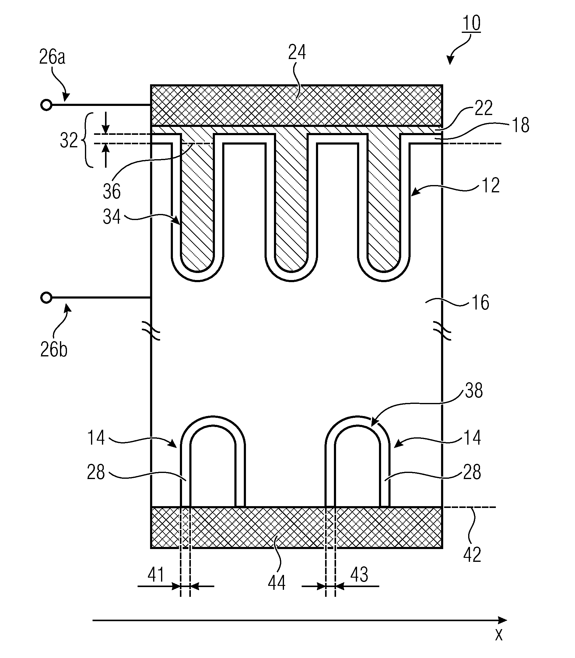
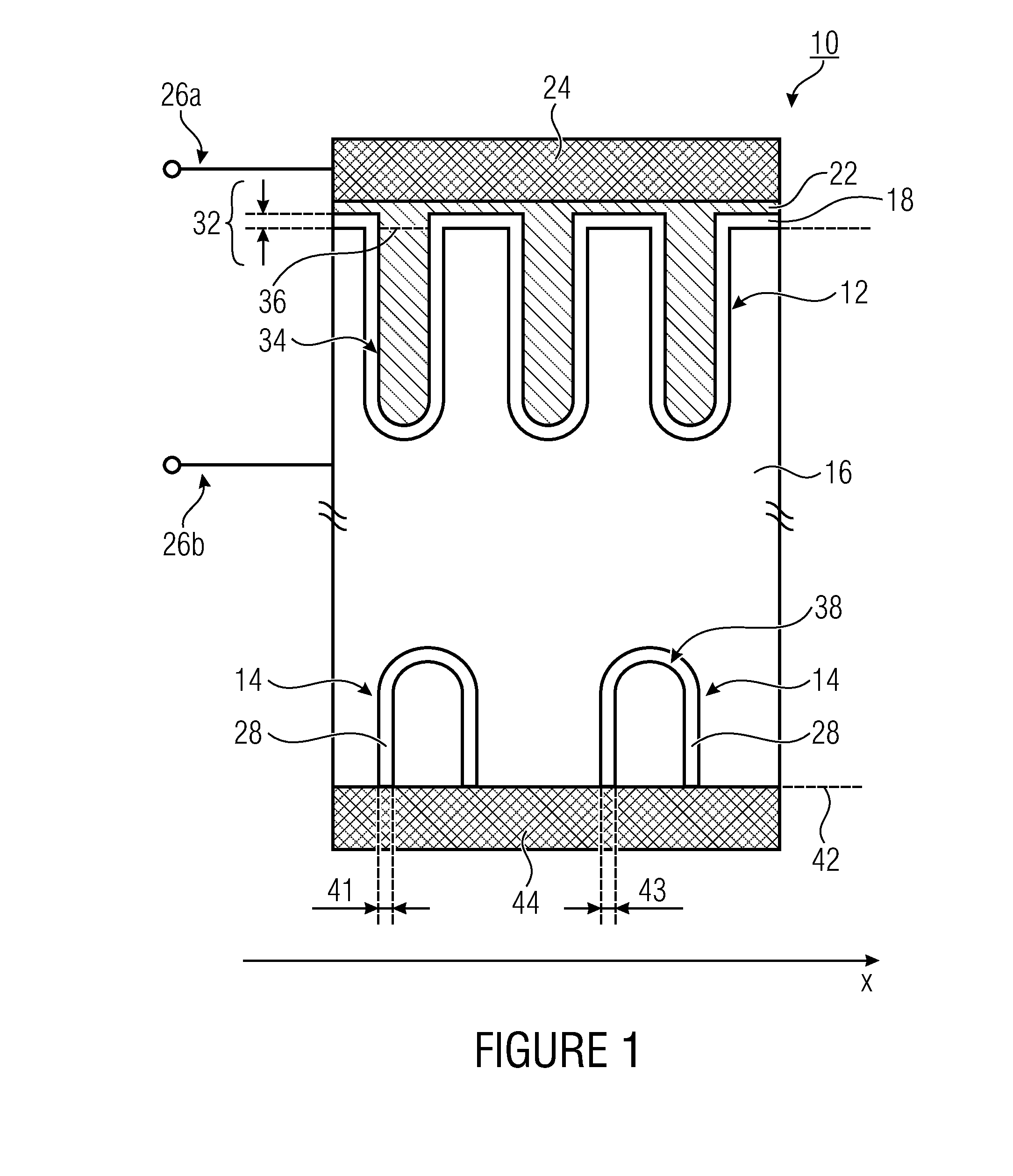
[0038]Before embodiments of the present invention will be discussed in detail below with reference to the drawings, it should be noted that identical, functionally equal or equal elements, objects and / or structures in the different figures are provided with the same reference numbers, so that the description of these elements illustrated in different embodiments is interchangeable or can be applied to each other.

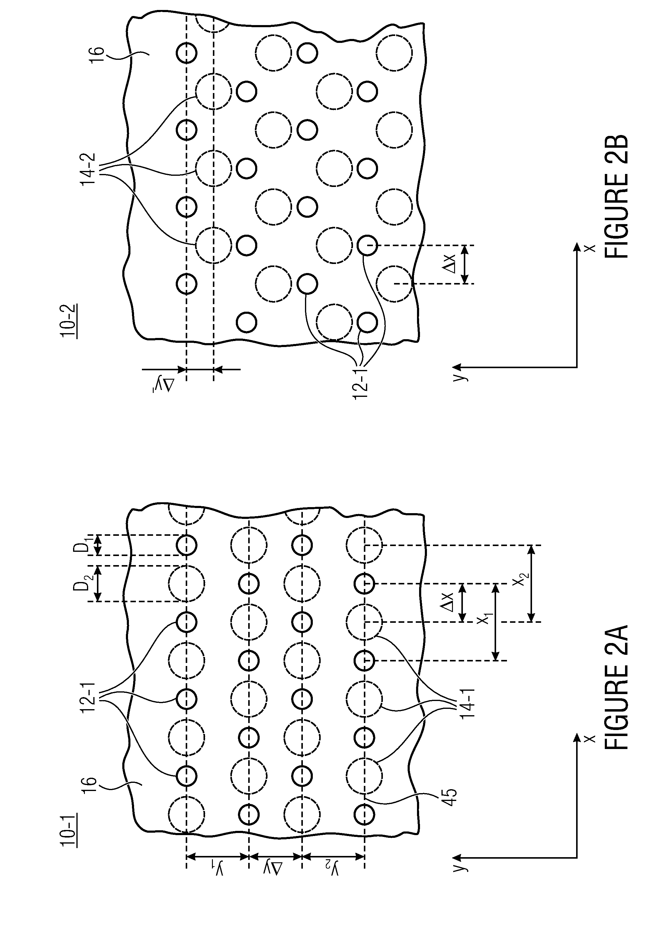
[0039]FIG. 1 shows a section of a schematic side view of an integrated capacitor 10 with a capacitor structure 12 and a compensation structure 14. The section can, for example, be part of a substrate from which a plurality of integrated capacitors 10 are formed. The capacitor structure 12 is integrated in a first main surface area of a substrate 16. The substrate 16 is, for example, a semiconductor material or a semiconductor substrate, such as based on silicon or of silicon, and can be implemented as a wafer from which the plurality of capacitors are formed. The substrate c...


PUM


Abstract

An integrated capacitor includes a substrate with a first main surface area and an opposing second main surface area. A capacitor structure with a dielectric layer is integrated in the first main surface area. A compensation structure with a compensation layer is integrated in the second main surface area. The ratio between a surface enlargement of the second main surface area effected by the compensation structure corresponds to at least 30% of the surface enlargement of the first main surface area effected by the capacitor structure.

Description

CROSS-REFERENCE TO RELATED APPLICATIONS[0001]This application claims priority from German Patent Application No. 102013019912.3, which was filed on Nov. 22, 2013, and is incorporated herein in its entirety by reference.BACKGROUND OF THE INVENTION[0002]The present invention relates to an integrated electric capacitor having a capacitor structure and a compensation structure and a method for producing the same. In particular, the present invention relates to trench capacitors structured on both sides for power-electronic applications.[0003]During manufacturing processes of integrated circuits, mechanical tensions can occur in the semiconductor material, which can interfere or affect the production process itself (for example, due to bending of the wafer) or can also affect the electric characteristics of the integrated circuit in a spurious manner. Frequently, there is a connection, for example between the structures and thicknesses of deposited insulating layers (e.g. dielectrics) an...

Claims


Application Information

Patent Timeline
Patent Type & Authority Patents(United States)
IPC IPC(8): H01L21/02H01L29/94H01L27/08H01L27/06H01L29/66H01L21/283H10N97/00
CPCH01L21/283H01L27/0682H01L27/0694H01L27/0805H01L29/66181H01L29/945H01L28/60
Inventor BAUERERLBACHER, TOBIASSCHWARZMANN, HOLGER
Owner FRAUNHOFER GESELLSCHAFT ZUR FOERDERUNG DER ANGEWANDTEN FORSCHUNG EV
Learn More