Supercharge Your Innovation With Domain-Expert AI Agents!

Semiconductor device

a technology of semiconductors and devices, applied in the direction of semiconductor devices, basic electric elements, electrical equipment, etc., can solve the problems of increasing the possibility of breakdown, and achieve the effect of improving the breakdown resistance and yield, and simplifying the manufacturing process

Active Publication Date: 2016-09-27
MITSUBISHI ELECTRIC CORP
View PDF23 Cites 1 Cited by
  • Summary
  • Abstract
  • Description
  • Claims
  • Application Information

AI Technical Summary

Benefits of technology

The solution simplifies the manufacturing process, enhances breakdown resistance, and prevents ohmic defects by reducing carrier concentration and improving solder adhesion, resulting in improved yield and reduced temperature during recovery operations.

Problems solved by technology

The recovery currents are therefore concentrated on an end portion of the p+-type anode layer to strengthen the electric field and increase the temperature thereof, thereby increasing the possibility of breakdown.

Method used


Image

  • Semiconductor device
  • Semiconductor device
  • Semiconductor device

Examples


embodiment 1

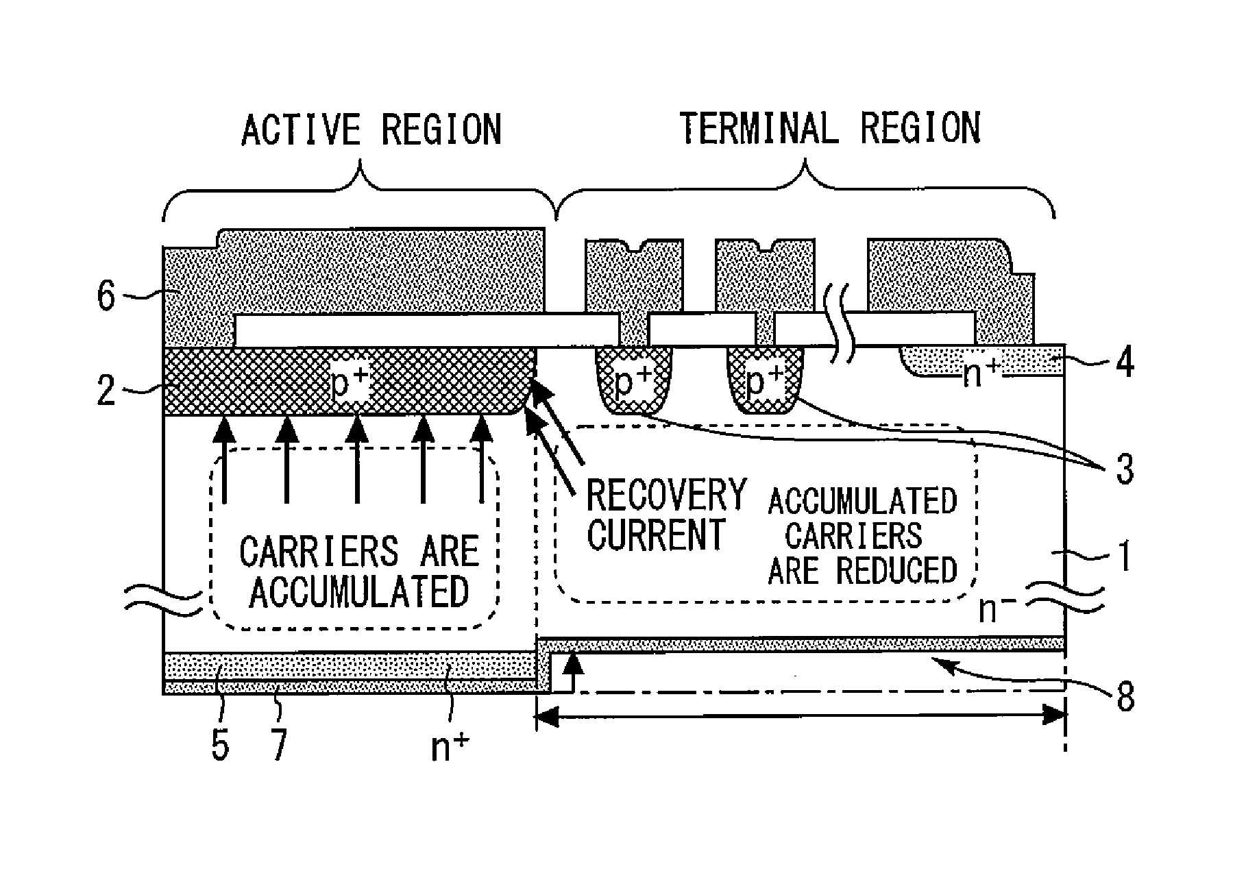
[0016]FIG. 1 is a sectional view of a semiconductor device according to Embodiment 1 of the present invention. An n−-type semiconductor substrate 1 has an active region and a terminal region disposed outside the active region. In a portion of an upper surface of the n−-type semiconductor substrate 1 (drift layer) in the active region, a p+-type anode layer 2 is formed.

[0017]In the upper surface of the n+-type semiconductor substrate 1 in the terminal region, a plurality of floated p+-type guard ring layers 3 are formed. The plurality of p+-type guard ring layers 3 are disposed outward from an end portion of the p+-type anode layer 2 and have a function to weaken an electric field at the end portion of the p+-type anode layer 2.

[0018]An n+-type channel stopper layer 4 is formed in an outermost peripheral portion of the upper surface of the n−-type semiconductor substrate 1. An n+-type cathode layer 5 having an impurity concentration higher than that in the n−-type semiconductor subst...

embodiment 2

[0025]FIG. 5 is a sectional view of a semiconductor device according to Embodiment 2 of the present invention. In the terminal region, not only the n+-type cathode layer 5 but also the n−-type semiconductor substrate 1 is trenched to an intermediate position, thereby forming the recess 8. The volume of the n−-type semiconductor substrate 1 in the terminal region is thereby reduced. Thus, the amount of accumulated carriers can be further reduced to achieve a further improvement in breakdown resistance. The effect is improved if the recess 8 is deeper. Accordingly, the depth of the recess 8 is adjusted according to a withstand voltage specification.

embodiment 3

[0026]FIG. 6 is a sectional view of a semiconductor device according to Embodiment 3 of the present invention. The recess 8 extends not only through the terminal region but also to an intermediate position in the active region (right below the pt-type anode layer 2). Recovery currents concentrated on the end portion of the p+-type anode layer 2 can be further reduced thereby. A further improvement in breakdown resistance can thus be achieved. The effect is improved if the width of the recess 8 is larger. Accordingly, the width of the recess 8 is adjusted according to a VF characteristic specification.


PUM


Abstract

An n−-type semiconductor substrate (1) includes an active region and a terminal region disposed outside the active region. A p+-type anode layer (2) is formed in a portion of an upper surface of the n−-type semiconductor substrate (1) in the active region. A plurality of p+-type guard ring layers (3) are formed in a portion of the upper surface of the n−-type semiconductor substrate (1) in the terminal region. An n+-type cathode layer (5) is formed in a lower surface of the n−-type semiconductor substrate (1). An anode electrode (6) is connected to the p+-type anode layer (2). A metallic cathode electrode (7) is connected to the n+-type cathode layer (5). A recess (8) is formed by trenching the n+-type cathode layer (5) in the terminal region. The cathode electrode (7) is also formed in the recess (8).

Description

TECHNICAL FIELD[0001]The present invention relates to a semiconductor device such as a diode for use in a power module.BACKGROUND ART[0002]When a current is caused to flow in a forward direction between a p+-type anode layer and an n+-type cathode layer in a diode, a large number of carriers are accumulated in an n−-type drift layer. Thereafter, when a switch is turned off, the accumulated carriers are discharged and recovery currents (reverse recovery currents) flow. During recovery operation, both the carriers accumulated in an active region and the carriers accumulated in a terminal region flow into the p+-type anode layer. The recovery currents are therefore concentrated on an end portion of the p+-type anode layer to strengthen the electric field and increase the temperature thereof, thereby increasing the possibility of breakdown. A diode having a recess formed by trenching the n+-type cathode layer in the terminal region to prevent this phenomenon has been proposed (see, for ...

Claims


Application Information

Patent Timeline
Patent Type & Authority Patents(United States)
IPC IPC(8): H01L29/861H01L29/08H01L29/739H01L29/66H01L29/06
CPCH01L29/861H01L29/0619H01L29/0638H01L29/0661H01L29/0696H01L29/0834H01L29/7395H01L29/8611H01L2924/12036H01L29/402H01L29/1602H01L29/1608H01L29/2003
Inventor OTSUKI, EIKOSADAMATSU, KOJIYOSHIURA, YASUHIRO
Owner MITSUBISHI ELECTRIC CORP
Features
  • R&D
  • Intellectual Property
  • Life Sciences
  • Materials
  • Tech Scout
  • Unparalleled Data Quality
  • Higher Quality Content
  • 60% Fewer Hallucinations
Learn More