Method for forming film having low resistance and shallow junction depth

a technology of low resistance and shallow junction depth, which is applied in the direction of coatings, metallic material coating processes, chemical vapor deposition coatings, etc., can solve the problems of reducing rs at shallow regions (e.g., xj10 nm) and not being successful

Active Publication Date: 2016-10-25
ASM IP HLDG BV
View PDF1342 Cites 324 Cited by
  • Summary
  • Abstract
  • Description
  • Claims
  • Application Information

AI Technical Summary

Problems solved by technology

However, reducing Rs at shallow regions (e.g., Xj<10 nm) has not been successful.

Method used


Image

  • Method for forming film having low resistance and shallow junction depth
  • Method for forming film having low resistance and shallow junction depth
  • Method for forming film having low resistance and shallow junction depth

Examples


examples

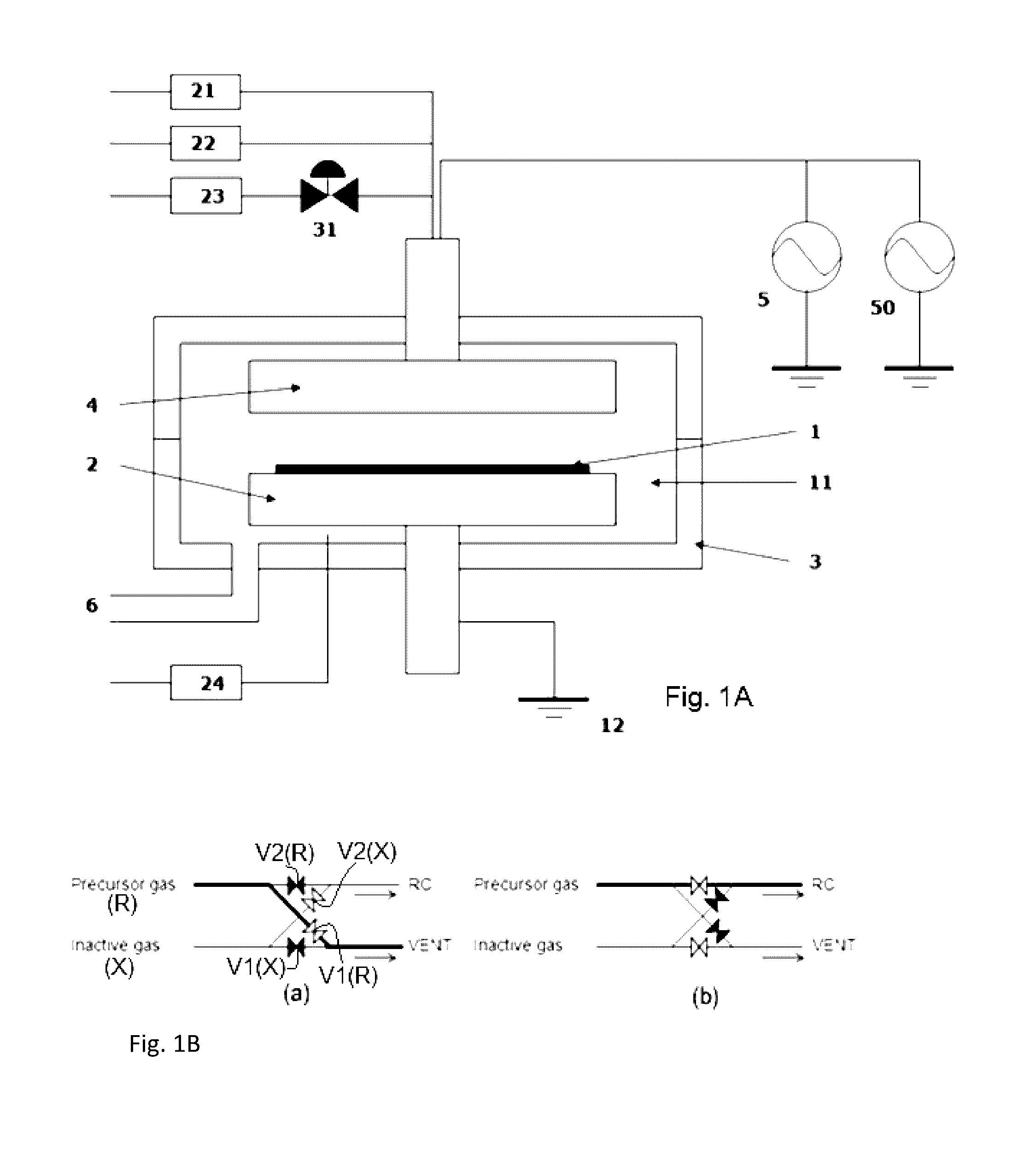
[0063]An arsenosilicate glass (ASG) film was formed on a Si substrate (Φ300 mm) by PEALD, one cycle of which was conducted under the conditions shown in Table 5 below using the PEALD apparatus illustrated in FIG. 1A (including a modification illustrated in FIG. 1B) with the sequence illustrated in FIG. 3.

[0064]

TABLE 5(the numbers are approximate)Conditions for ASG Film DepositionSubstrate temperature300° C.Pressure400 PaSilicon precursorbis(diethylamino)silane (BDEAS)Silicon precursor pulse0.3 secSilicon precursor purge0.8 secDopant precursorArsenic triethoxideDopant precursor pulse0.3 secDopant precursor purge5.0 secReactantO2Flow rate of reactant500 sccm(continuous)Dilution gas (rare gas)ArFlow rate of dilution gas2200 sccm(continuous)RF power (13.56 MHz) for a200 W300-mm waferRF power pulse0.4. secPurge upon the RF power pulse0.1 secThickness of film5 nm

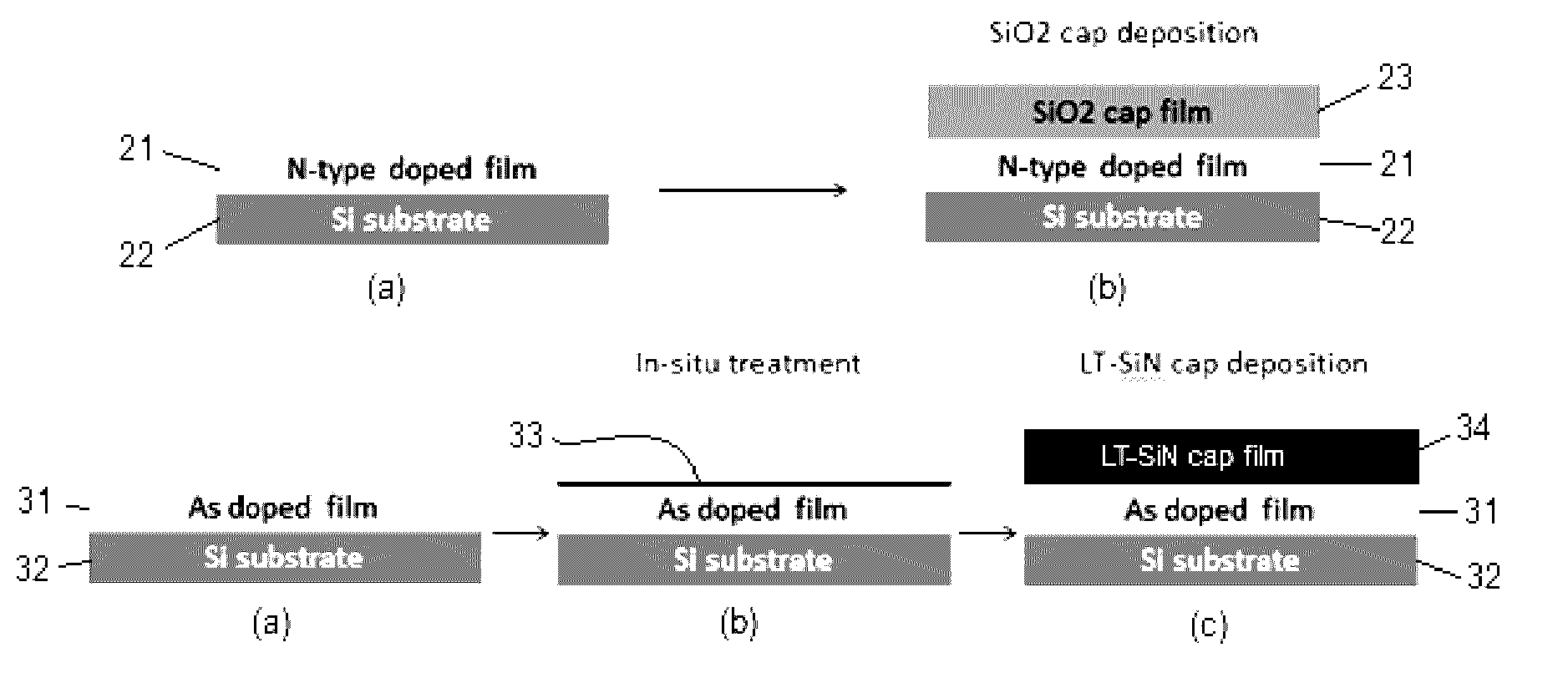
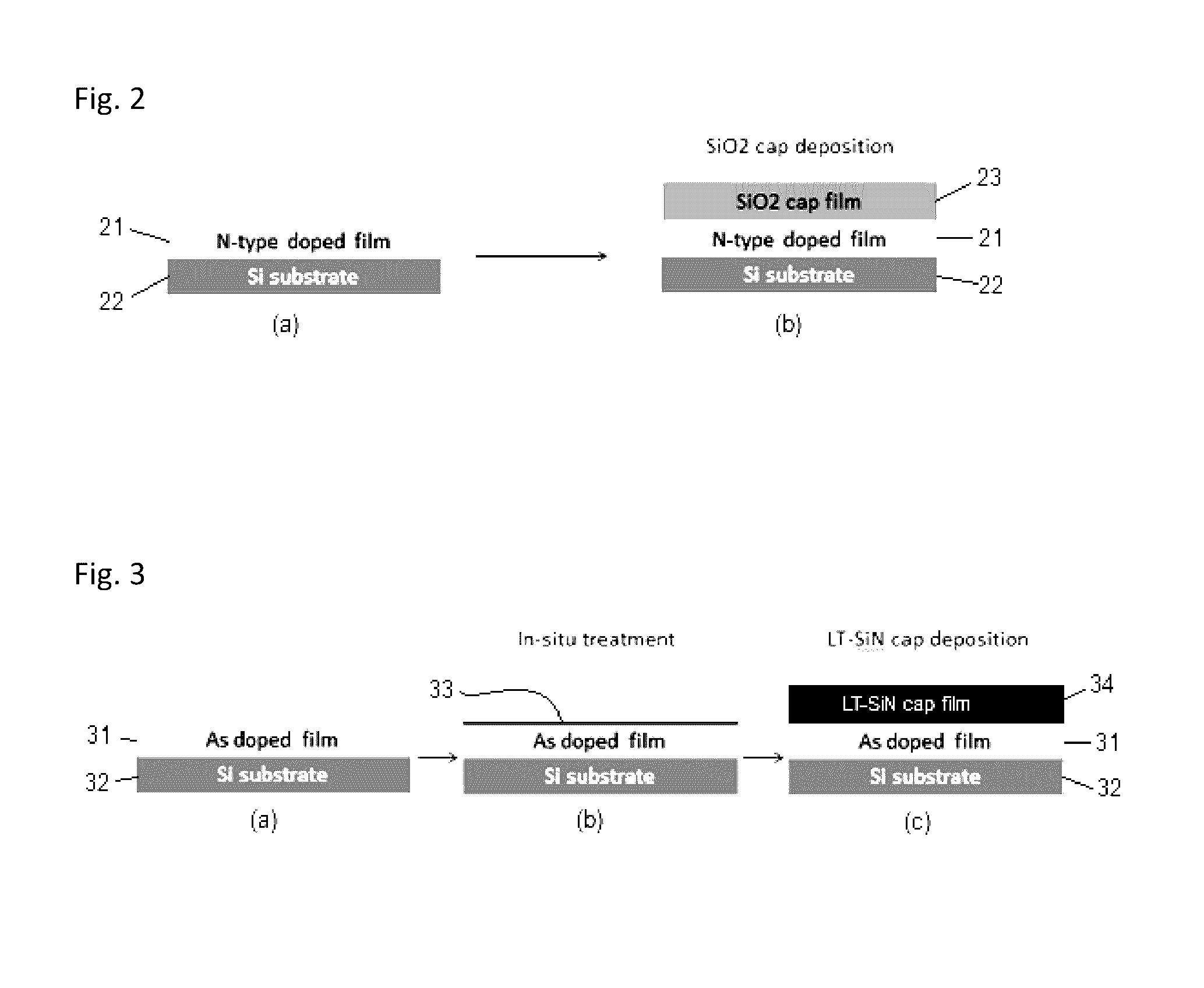
[0065]The dopant layer was treated in situ with a treating gas under conditions shown in Table 6 below in the same apparatus.

[00...


PUM

PropertyMeasurementUnit
temperatureaaaaaaaaaa
thicknessaaaaaaaaaa
temperatureaaaaaaaaaa

Abstract

A method for forming on a substrate a doped silicon oxide film with a cap film, includes: forming an arsenosilicate glass (ASG) film as an arsenic (As)-doped silicon oxide film on a substrate; continuously treating a surface of the ASG film with a treating gas constituted by Si, N, and H without excitation; and continuously forming a silicon nitride (SiN) film as a cap film on the treated surface of the ASG film.

Description

BACKGROUND OF THE INVENTION[0001]1. Field of the Invention[0002]The present invention relates generally to a method for forming on a substrate an arsenosilicate glass (ASG or AsSG) film with a cap film.[0003]2. Related Art[0004]Metal-oxide-semiconductor field effect transistors (MOSFETs) are fundamental switching devices to perform logic operations in large scale integrated circuits (LSIs). As the downsizing of MOSFETs progress, decrease in junction depth (Xj) and increase in doping concentration are indispensable in the scaling trend. FinFETs and Tri-gate FETs have fin structures for source / drain extension, and such devices require reduction of lateral resistance (or sheet resistance) of the source / drain extension regions to obtain larger drain current by scaling down of MOSFETs. Therefore, both shallow Xj (Xj is defined as the depth where dopant concentration is 5×10¹⁸ / cm3) and low sheet resistance (Rs) of the source / drain extension regions are indispensable for further scaling do...

Claims


Application Information

Patent Timeline
Patent Type & Authority Patents(United States)
IPC IPC(8): H01L21/31H01L21/02
CPCH01L21/0228H01L21/0217H01L21/02142H01L21/02274H01L21/02337C23C16/345C23C16/401C23C16/45531C23C16/45538H01L21/02126H01L21/022H01L21/02211H01L21/02219
Inventor KIMURA, YOSUKEDE ROEST, DAVID
Owner ASM IP HLDG BV
Why Eureka
Try Eureka