Method for fabricating semiconductor device

a technology of semiconductor devices and gate electrodes, which is applied in the direction of semiconductor devices, electrical equipment, transistors, etc., can solve the problems of insufficient efficiency of using doped polysilicon gate electrodes to improve threshold voltage, and achieve the effect of enhancing the working performance of transistors and increasing the production yield of transistors

Active Publication Date: 2016-11-08
UNITED MICROELECTRONICS CORP
View PDF45 Cites 0 Cited by
  • Summary
  • Abstract
  • Description
  • Claims
  • Application Information

AI Technical Summary

Benefits of technology

[0005]Therefore, the object of the present invention is to provide a method for fabricating a semiconductor device in order to improve the working performance of a field effect transistor and increase the production yield thereof.
[0022]The present invention provides an improved method for fabricating a semiconductor device. In the later stage of removing the dummy gate electrode layer, an ammonium hydroxide treatment process is performed to minimize the residual dummy gate electrode layer, so that the working function layer between the gate oxide layer and the metal gate electrode formed in the subsequent process has a satisfactory working function value to meet the electrical requirements of the metal gate electrode. In such way, the working performance of the transistor is enhanced and the production yield of the transistor is increased.

Problems solved by technology

Moreover, since the doping capacity of the conventional polysilicon gate electrode is limited, the efficacy of using the doped polysilicon gate electrode to improve the threshold voltage is usually insufficient.
However, it is still a challenge for those skilled in the art to increase the working performance and the production yield of the field effect transistor.

Method used


Image

  • Method for fabricating semiconductor device
  • Method for fabricating semiconductor device
  • Method for fabricating semiconductor device

Examples


Embodiment Construction

[0027]The present invention will now be described more specifically with reference to the following embodiments. It is to be noted that the following descriptions of preferred embodiments of this invention are presented herein for purpose of illustration and description only. It is not intended to be exhaustive or to be limited to the precise form disclosed.

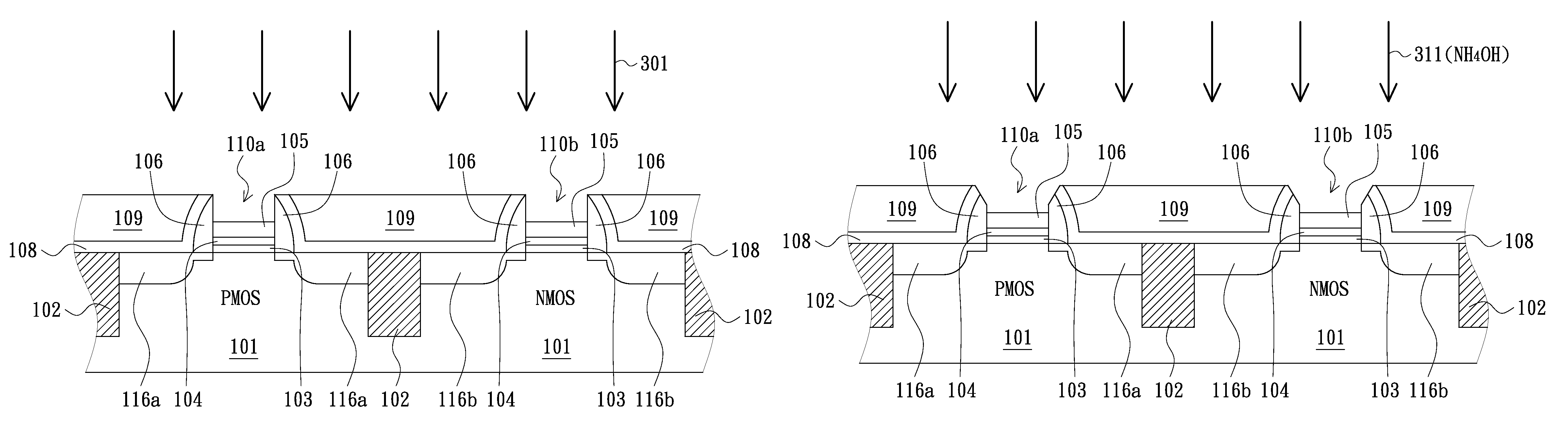
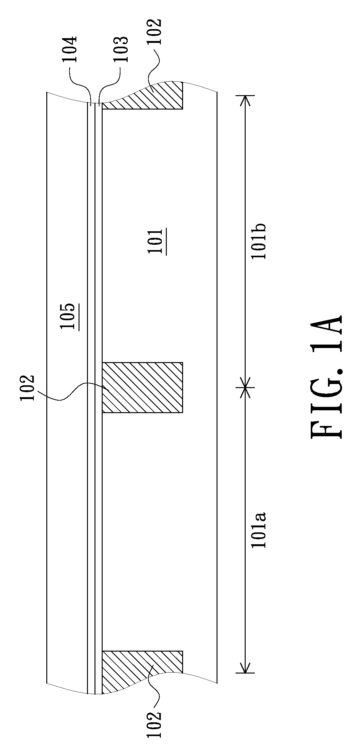
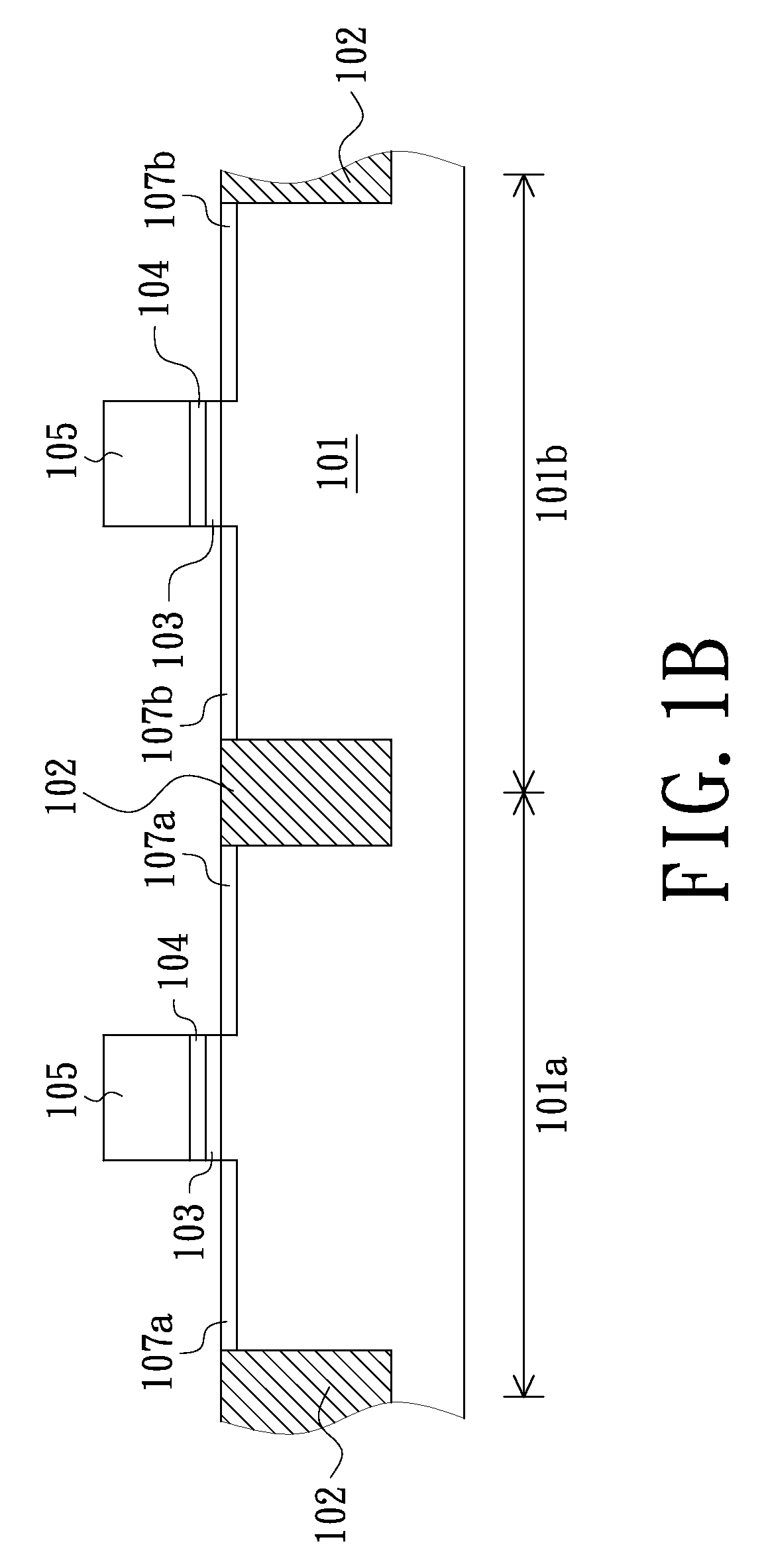
[0028]The present invention provides an improved method for fabricating a field effect transistor (FET) with enhanced working performance and production yield. The above and other objects, features and advantages of the present invention will become more readily apparent to those ordinarily skilled in the art after reviewing the following detailed description and accompanying drawings. An example of the present invention will be illustrated by referring to a method for fabricating a complementary metal-oxide-semiconductor (CMOS) device. Nevertheless, the present invention is not limited to a method for fabricating the CMOS device...


PUM


Abstract

A method for fabricating a semiconductor device includes the following steps. Firstly, a dummy gate structure having a dummy gate electrode layer is provided. Then, the dummy gate electrode layer is removed to form an opening in the dummy gate structure, thereby exposing an underlying layer beneath the dummy gate electrode layer. Then, an ammonium hydroxide treatment process is performed to treat the dummy gate structure. Afterwards, a metal material is filled into the opening.

Description

FIELD OF THE INVENTION[0001]The present invention relates to a method for fabricating a semiconductor device, and more particularly to a method for fabricating a field effect transistor (FET) with a metal gate structure.BACKGROUND OF THE INVENTION[0002]As the demand on the device integration of an integrated circuit is gradually increased, the feature size of a semiconductor device (e.g. a field effect transistor) becomes smaller and smaller, and the thickness of a gate oxide layer of the field effect transistor is reduced. For maintaining the dielectric performance and reducing current leakage, the gate oxide layer of the semiconductor device is usually made of a high-k material. Moreover, since the doping capacity of the conventional polysilicon gate electrode is limited, the efficacy of using the doped polysilicon gate electrode to improve the threshold voltage is usually insufficient. Nowadays, for solving the problems resulting from reduction of the device feature size, the pol...

Claims


Application Information

Patent Timeline
Patent Type & Authority Patents(United States)
IPC IPC(8): H01L21/3205H01L29/423H01L21/3213H01L21/28H01L21/8238H01L29/66H01L29/49H01L29/51H01L29/78
CPCH01L29/6659H01L21/28088H01L21/32134H01L21/823842H01L29/42376H01L29/4966H01L29/66545H01L29/513H01L29/517H01L29/518H01L29/7833
Inventor LAI, CHIEN-MINGCHEN, YI-WENLEE, ZHI-CHENGHUANG, TONG-JYUNHSU, CHE-HUALIN, KUN-HSIENLEE, TZUNG-YINGHSU, CHI-MAOHUANG, HSIN-FULIN, CHIN-FU
Owner UNITED MICROELECTRONICS CORP
Why Eureka
Try Eureka