Hybrid integrated optical device enabling high tolerance optical chip bonding and the method to make the same

a hybrid optical and chip technology, applied in the direction of optical waveguide light guide, instruments, optics, etc., can solve the problems of harming device performance, requiring high accuracy in the alignment of in-plane direction perpendicular to optical propagation, and the final alignment error, so as to increase the alignment tolerance

Active Publication Date: 2016-12-06
LAXENSE
View PDF12 Cites 1 Cited by
  • Summary
  • Abstract
  • Description
  • Claims
  • Application Information

AI Technical Summary

Benefits of technology

[0008]The optical devices according to embodiments of the present invention significantly increase the alignment tolerance between two optical chips in the in-plane direction perpendicular to optical propagation.

Problems solved by technology

However, unlike the mature integrated circuit (IC) fully automated packaging processes, assembling these optical chips requires very precise alignment, on the order of micrometer or less, because these chips and optical benches usually include tiny optical waveguides which must be well aligned with each other to form an optical transmission path.
A modern top-of-the-line flip-chip bonder can achieve a + / −0.5 micrometer alignment accuracy, however, in practice, the bonding involving processes, including thin film metal solder melting, adhesive curing, etc., inevitably contributing to final alignment error due to physical movement of the chip under temperature, stress or material phase change.
However, the alignment of in-plane direction perpendicular to optical propagation requires high accuracy, especially for small optical waveguides on the micrometer scale such as those in lasers.
However, including a taper structure as part of the optical waveguide requires design change of the optical chips which prohibits the use of widely available and proven commercial chips as well as, in many cases, harms device performance.
The lens which can be used in such condition cannot be made monolithically on the optical bench and has to be installed separately which introduces additional alignment error during the assembling.
These and similar methods have been proposed but none of them is being adopted in mass production due to above-stated issues.

Method used


Image

  • Hybrid integrated optical device enabling high tolerance optical chip bonding and the method to make the same
  • Hybrid integrated optical device enabling high tolerance optical chip bonding and the method to make the same
  • Hybrid integrated optical device enabling high tolerance optical chip bonding and the method to make the same

Examples


Embodiment Construction

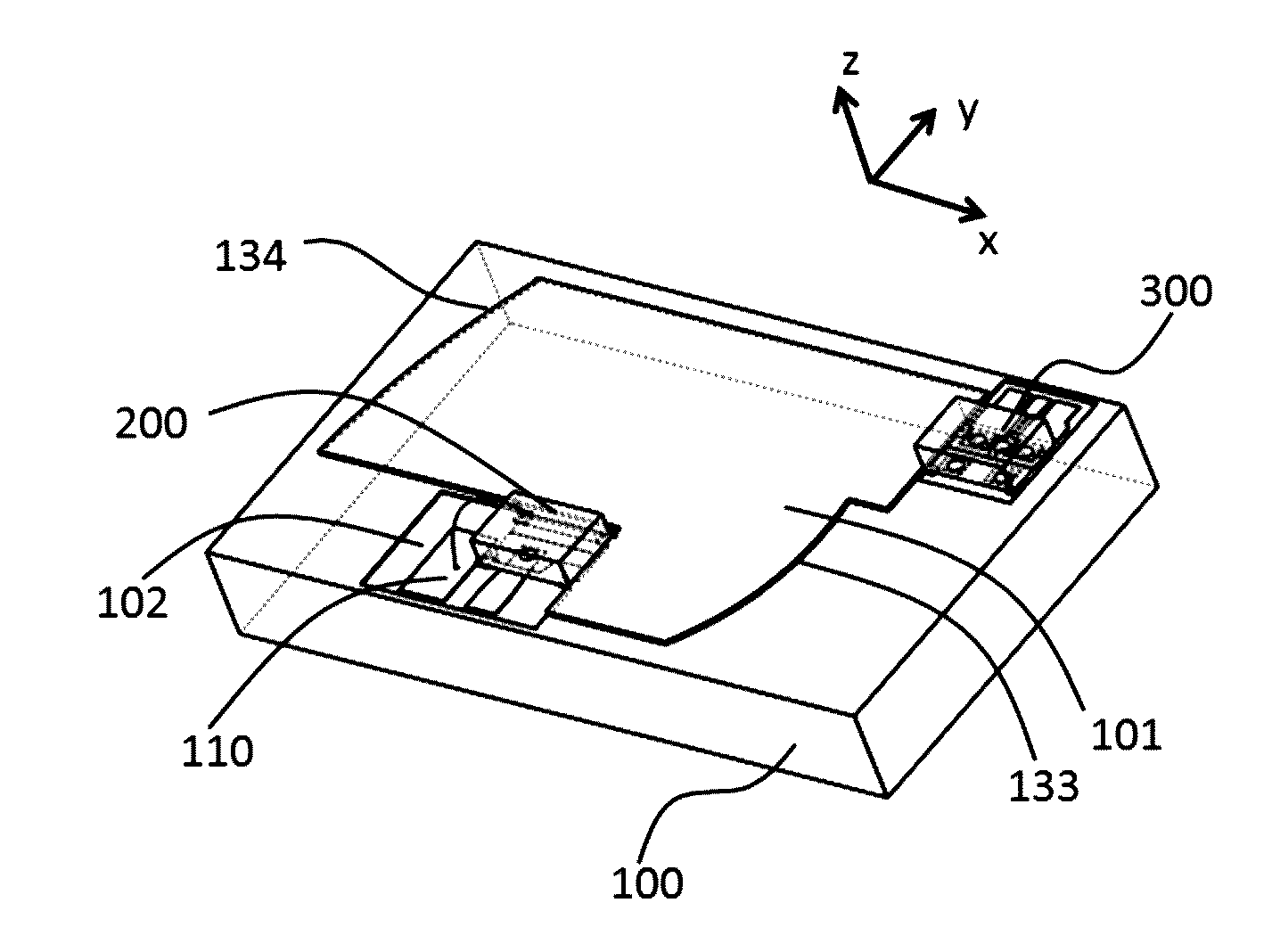
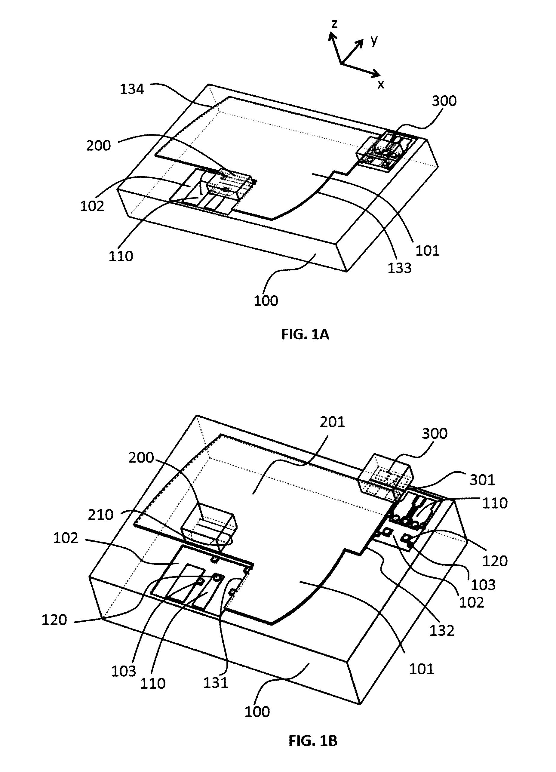
[0024]An embodiment of the present invention is described with reference to FIGS. 1A-1B. The optical device includes an optical bench with at least one large area slab optical waveguide, an etched trench, spacers, metal traces and micro solders; a flip-chip bonded first optical chip with at least one optical waveguide; and a flip-chip bonded second optical chip with at least one optical waveguide. FIG. 1A is a perspective view illustrating the hybrid integrated optical device while FIG. 1B is an exploded view. The components are drawn in a way as if they were transparent for the purpose of easy observation of structures behind (structures behind other structures are shown in dashed lines). The hybrid integrated optical device includes an optical bench 100, a flip-chip bonded first optical chip 200 and a flip-chip bonded second optical chip 300. The optical bench 100 can be made of any semiconductor or insulating materials including, but not limited to, silicon, silica, and indium ph...


PUM


Abstract

An optical device includes an optical bench and two flip-chip bonded optical chips. The optical bench includes a large area slab waveguide structure which has an input facet facing the first optical chip, an output facet facing the second optical chip, and one or more curved facet which reflects the slab mode light such that the input optical mode coupled through the input facet diverges in the slab waveguide plane as it propagates, reflects at the one or more curved facets, and focuses to an output optical mode at the output facet with mode size larger than the input optical mode in the in-plane direction. During fabrication, after the first optical chip is flip-chip bonded, the location of the focused output optical mode on the output facet is determined, and then the second optical chip is flip-chip bonded based on the determined location of the output optical mode.

Description

BACKGROUND OF THE INVENTION[0001]Field of the Invention[0002]The invention relates to an optical device with hybrid integrated optical waveguide chips. In particular, the invention relates to an optical device using passively aligned flip-chip bonding method to hybrid integrate two optical waveguide chips with different optical waveguide mode size on an optical bench which reduces the required bonding alignment accuracy through its specially designed slab waveguide structures.[0003]Description of Related Art[0004]Optical interconnects are adopted in data communications at unprecedented rate as more bandwidth and longer transmission reach are required by mega datacenters for applications from social networks, cloud service, to big data analysis and high performance computing. Unlike optical transceiver modules or subsystems made of ultrahigh performance discrete components in telecommunications, lower cost, more compact and more power efficient optical transceivers or engines are dem...

Claims


Application Information

Patent Timeline
Patent Type & Authority Patents(United States)
IPC IPC(8): G02B6/12G02B6/136
CPCG02B6/12002G02B6/12004G02B6/136G02B2006/12152G02B2006/12061G02B2006/12078G02B6/4237G02B6/4244G02B6/4257G02B6/43G02B6/264
Inventor SUN, XIAOCHENFENG, NINGNING
Owner LAXENSE
Why Eureka
Try Eureka