Method of fabricating optoelectronic integrated circuit chip

Inactive Publication Date: 2005-08-04
ELECTRONICS & TELECOMM RES INST
View PDF2 Cites 0 Cited by
  • Summary
  • Abstract
  • Description
  • Claims
  • Application Information

AI Technical Summary

Benefits of technology

[0013] The present invention is directed to a method of fabricating an optoelectronic integrated circuit chip, in which an optical absorption layer of a wave-guide type optical detector is formed by using a selective area growth by MOCVD to be thicker than a collector layer of a hetero-junction bipolar transistor, thereby enhancing quantum efficiency and increasing alignment tolerance with an optic fiber.
[0014] The present invention is also directed to a method of fabricating an optoelectronic integrated circuit chip, in which a ultra-high speed wave-guide type optical detector including a thick optical absorption layer formed by using a selective area growth by MOCVD and having high quantum efficiency, and a hetero-junction bipolar transistor are integrated as a single chip on a semi-insulated InP substrate, so that light is converted into an electrical signal by the wave-guide type optical detector, and the converted electrical signal is amplified by the high gain hetero-junction bipolar transistor having a crystal layer structure of n+InP / p+InGaAs / n−InGaAs / n+InGaAs integrated together with the wave-guide type optical detector as a single chip on the semi-insulated InP substrate, thereby enhancing receiver sensitivity and detection speed.

Problems solved by technology

Thus, the optical communication system should include a front end receiver having a complicated optoelectronic circuit for detecting and amplifying the ultra high speed optical signal, so that the manufacturing cost is increased.
Consequently, it is difficult to economically fabricate an optical receiver with an excellent sensitivity.

Method used


Image

  • Method of fabricating optoelectronic integrated circuit chip
  • Method of fabricating optoelectronic integrated circuit chip
  • Method of fabricating optoelectronic integrated circuit chip

Examples


Embodiment Construction

[0021] The present invention will now be described more fully hereinafter with reference to the accompanying drawings, in which preferred embodiments of the invention are provided so that this disclosure will be thorough and complete, and will fully convey the scope of the invention to those skilled in the art.

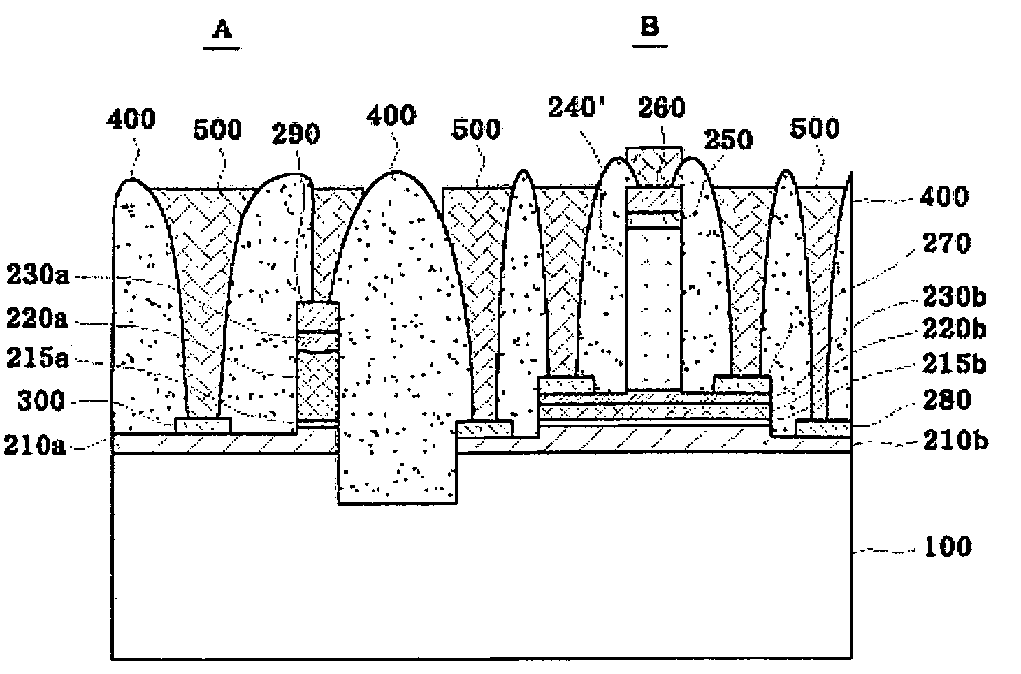
[0022]FIG. 2 is a cross-sectional view of an optoelectronic integrated circuit chip according to an embodiment of the present invention.

[0023] Referring to FIG. 2, a wave-guide type optical detector A and a hetero-junction bipolar transistor B are integrated as a single chip on a semi-insulated InP substrate 100.

[0024] The wave-guide type optical detector A includes an n+InGaAs layer 210a, an n−InP layer 215a, an n−InGaAs optical absorption layer 220a, and a p+InGaAs ohmic layer 230a, which are sequentially stacked on a predetermined region of the semi-insulated InP substrate 100. Here, the n−InGaAs optical absorption layer 220a and the p+InGaAs ohmic layer 230a are formed ...


PUM


Abstract

Provided is a method of fabricating an optoelectronic integrated circuit chip. In particular, a method of fabricating an optoelectronic integrated circuit chip is provided, in which an optical absorption layer of a wave-guide type optical detector is grown to be thicker than a collector layer of a hetero-junction bipolar transistor by using a selective area growth by metal organic chemical vapor deposition (MOCVD) method, and the wave-guide type optical detector and the hetero-junction bipolar transistor are integrated as a single chip on a semi-insulated InP substrate, thereby readily realizing the wave-guide type optical detector improved in quantum efficiency and having the ultra-high speed characteristics.

Description

CROSS-REFERENCE TO RELATED APPLICATION [0001] This application claims the benefit of Korea Patent Application Nos. 2003-94753 filed on Dec. 22, 2003 and 2004-57043 filed on Jul. 22, 2004, the disclosure of which is hereby incorporated herein by reference in its entirety. BACKGROUND OF THE INVENTION [0002] 1. Field of the Invention [0003] The present invention relates to a method of fabricating an optoelectronic integrated circuit chip, and more particularly, to a method of fabricating an optoelectronic integrated circuit chip, in which an optical absorption layer of a wave-guide type optical detector is formed to be thicker than a collector layer of a hetero-junction bipolar transistor by using a selective area growth by MOCVD (Metal Organic Chemical Deposition), and the wave-guide type optical detector and the hetero-junction bipolar transistor are integrated as a single chip on a semi-insulated InP substrate, thereby readily realizing the wave-guide type optical detector with an i...

Claims


Application Information

Patent Timeline
IPC IPC(8): H01L21/331H01L31/109H01L31/11
CPCH01L29/66318H01L31/1105H01L31/109
Inventor NAM, EUN SOOKIM, HO YOUNGOH, MYOUNG SOOKJUNG, DONG YUNHONG, SEON EUICHO, KYOUNG IK
Owner ELECTRONICS & TELECOMM RES INST
Why Eureka
Try Eureka