Magnetic-field and magnetic-field gradient sensors based on lateral SOI bipolar transistors

Inactive Publication Date: 2016-12-06
IBM CORP
View PDF12 Cites 1 Cited by
  • Summary
  • Abstract
  • Description
  • Claims
  • Application Information

AI Technical Summary

Benefits of technology

[0007]In an aspect of the present disclosure, there is a magnetic sensor device based on SOI lateral Bipolar Junctio

Problems solved by technology

In such applications, however, relatively large magnetic fields are needed to avoid interference/error by background magnetic fields, such as the Earth's magnetic field, fields from ferromagnetic objects, and electromagnetic interference (EMI).
While appearing to be competitive in the power-cost comparison, the AMR (anisotropic magnetoresistive) and GM

Method used


Image

  • Magnetic-field and magnetic-field gradient sensors based on lateral SOI bipolar transistors
  • Magnetic-field and magnetic-field gradient sensors based on lateral SOI bipolar transistors
  • Magnetic-field and magnetic-field gradient sensors based on lateral SOI bipolar transistors

Examples


Embodiment Construction

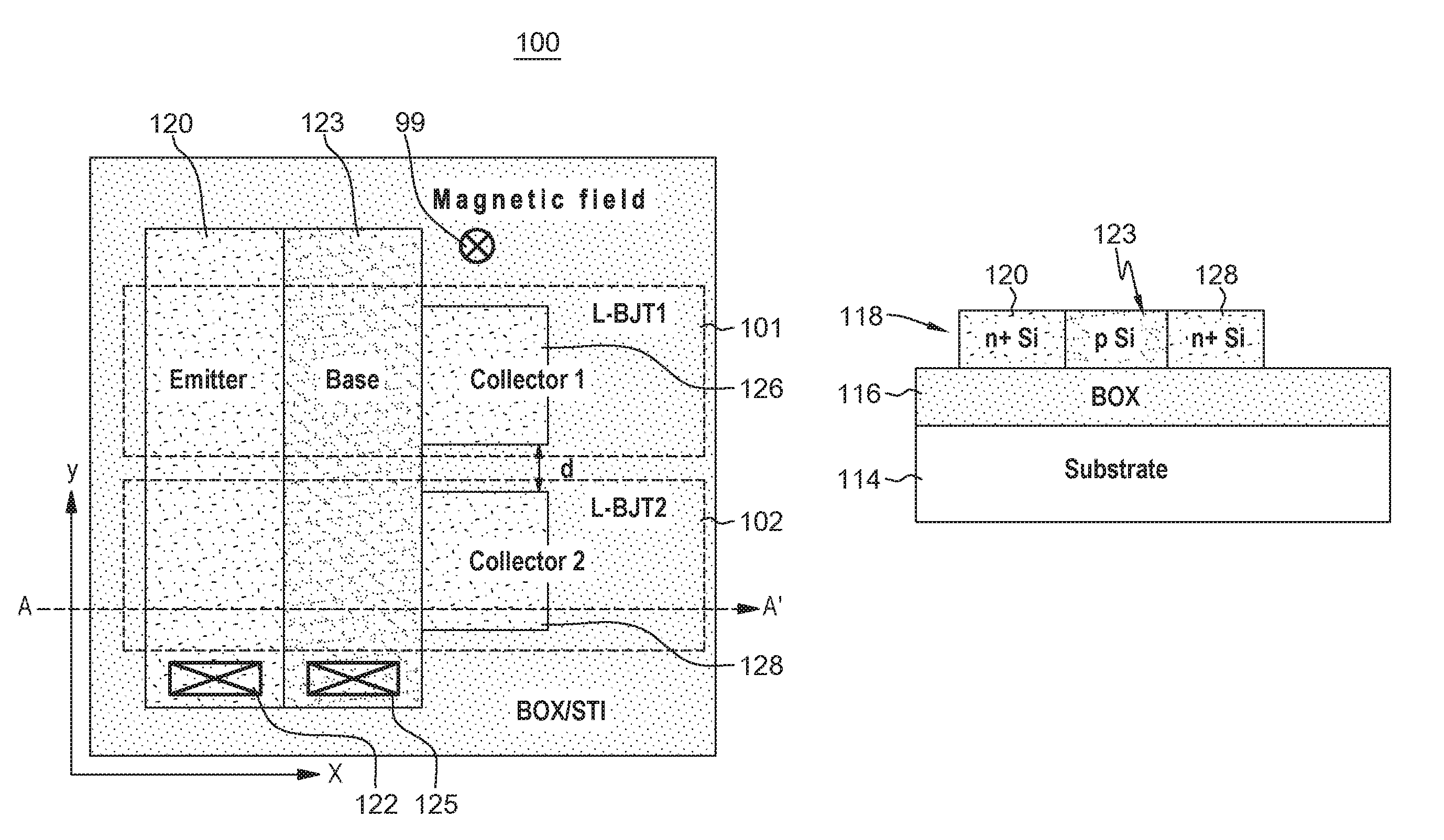
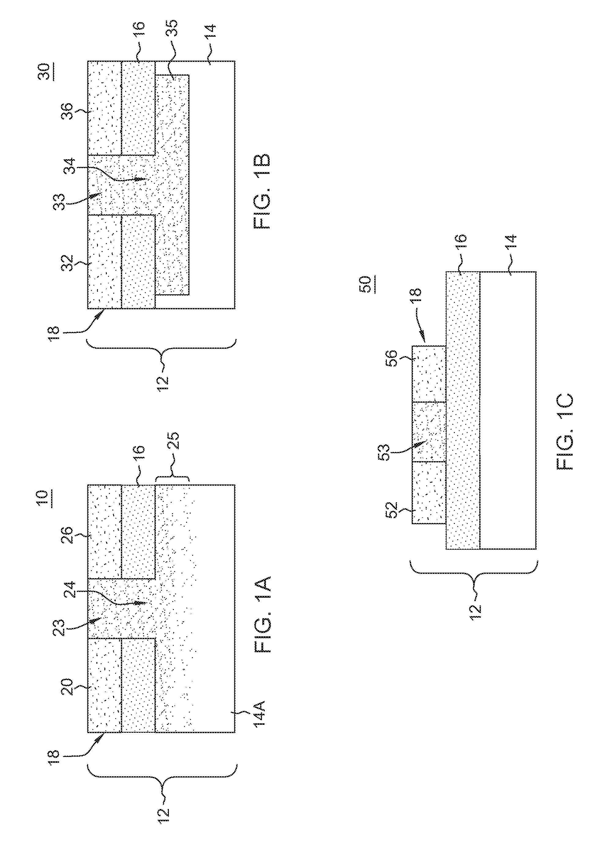
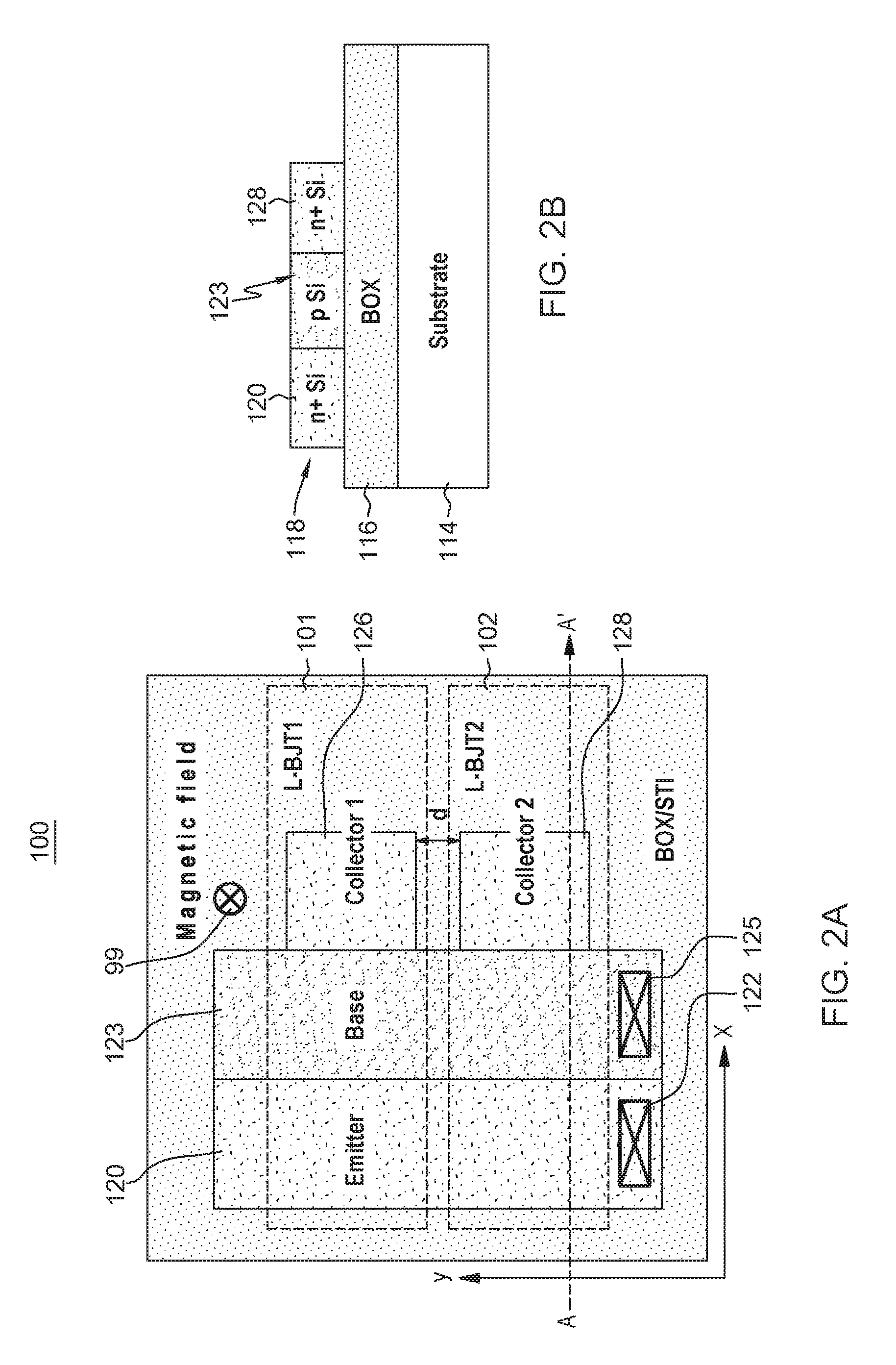
[0023]The present application will now be described in greater detail by referring to the following discussion and drawings that accompany the present application. It is noted that the drawings of the present application are provided for illustrative purposes and, as such, they are not drawn to scale. In the drawings and the description that follows, like elements are referred to by like reference numerals. For purposes of the description hereinafter, the terms “upper”, “lower”, “right”, “left”, “vertical”, “horizontal”, “top”, “bottom”, and derivatives thereof shall relate to the components, layers and / or elements as oriented in the drawing figures which accompany the present application.

[0024]In one embodiment, the disclosure provides a magnetic sensor based on a Silicon-on-insulator (SOI) lateral BJT that is free from the parasitic current as seen in the vertical bulk BJT counterpart. The structure of the SOI lateral BJT also allows flexible placement of terminal metal contacts t...


PUM


Abstract

A lateral bipolar junction transistor (BJT) magnetic field sensor that includes a layout of two or more adjacent lateral BJT devices. Each BJT includes a semiconductor base region of a first conductivity type doping, a semiconductor emitter region of a second conductivity type doping and laterally contacting the base region; and a first semiconductor collector region of a second conductivity type doping contacting said base region on an opposite side thereof. A second collector region of the second conductivity type doping is also formed contacting the base region on the opposite side thereof in spaced apart relation with the first collector region. The first adjacent lateral BJT device includes the emitter, base and first collector region and the second adjacent lateral BJT device includes the emitter, base and second collector region. The sensor induces a detectable difference in collector current amounts in the presence of an external magnetic field transverse to a plane defined by the layout.

Description

FIELD[0001]The present disclosure relates generally to magnetic sensor devices, and in particular magnetic sensor based on SOI lateral bipolar transistors and its method of manufacture.BACKGROUND[0002]Traditionally in industry, sensing of magnetic field is utilized for control and measurement of: linear and rotary position sensing, gear tooth sensing, and current sensing. In such applications, however, relatively large magnetic fields are needed to avoid interference / error by background magnetic fields, such as the Earth's magnetic field, fields from ferromagnetic objects, and electromagnetic interference (EMI).[0003]Solid-state magnetic sensors have received increasing attention given their inherent advantage in compactness and power efficiency when compared with traditional / complex counterparts such as search coil, flux gate, and superconducting quantum interference detectors (SQUID) and spin resonance magnetometers (the latter two usually need to be operated at low temperature fo...

Claims


Application Information

Patent Timeline
IPC IPC(8): G01R33/09H01L27/12G01R33/02H01L29/735H01L29/66H01L29/82
CPCH01L29/82H01L29/735H01L29/6625H01L27/1203G01R33/02H01L29/66265H01L29/7317H01L29/1008G01R33/0052G01R33/0058H10N50/01G01R33/09H01L29/0649H01L29/41708
Inventor NING, TAK H.YAU, JENG-BANG
Owner IBM CORP
Why Eureka
Try Eureka