Light-emitting element, display module, lighting module, light-emitting device, display device, electronic device, and lighting device

a technology of light-emitting elements and display modules, which is applied in the direction of semiconductor devices, solid-state devices, oled structures, etc., can solve the problems of large pixel size of displays and interference phenomena between adjacent pixels, and achieve high-quality images, suppress crosstalk generation, and high-quality images

Active Publication Date: 2016-12-06
SEMICON ENERGY LAB CO LTD
View PDF56 Cites 39 Cited by
  • Summary
  • Abstract
  • Description
  • Claims
  • Application Information

AI Technical Summary

Benefits of technology

[0017]In view of the above, it is an object of one embodiment of the present invention to provide a tandem light-emitting element in which generation of crosstalk can be suppressed even when the element is applied to a high-definition display.
[0051]According to one embodiment of the present invention, by using the above light-emitting element, a display module, a lighting module, a light-emitting device, a display device, an electronic device, and a lighting device each of which can display high-quality images and consumes low power can be provided.

Problems solved by technology

In the case of manufacturing a high-definition display by using a light-emitting element (hereinafter referred to as a tandem light-emitting element) as disclosed in Patent Document 1 in which a plurality of light-emitting units is separated from each other by a charge generation layer, problems which do not arise in lighting application or a display having a large pixel size are caused in some cases.
One of such problems is an interference phenomenon between adjacent pixels, that is, crosstalk.

Method used


Image

  • Light-emitting element, display module, lighting module, light-emitting device, display device, electronic device, and lighting device
  • Light-emitting element, display module, lighting module, light-emitting device, display device, electronic device, and lighting device
  • Light-emitting element, display module, lighting module, light-emitting device, display device, electronic device, and lighting device

Examples


embodiment 1

(Embodiment 1)

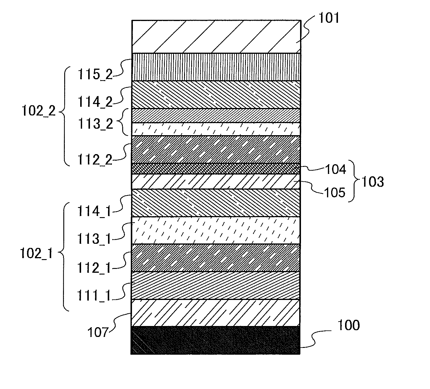
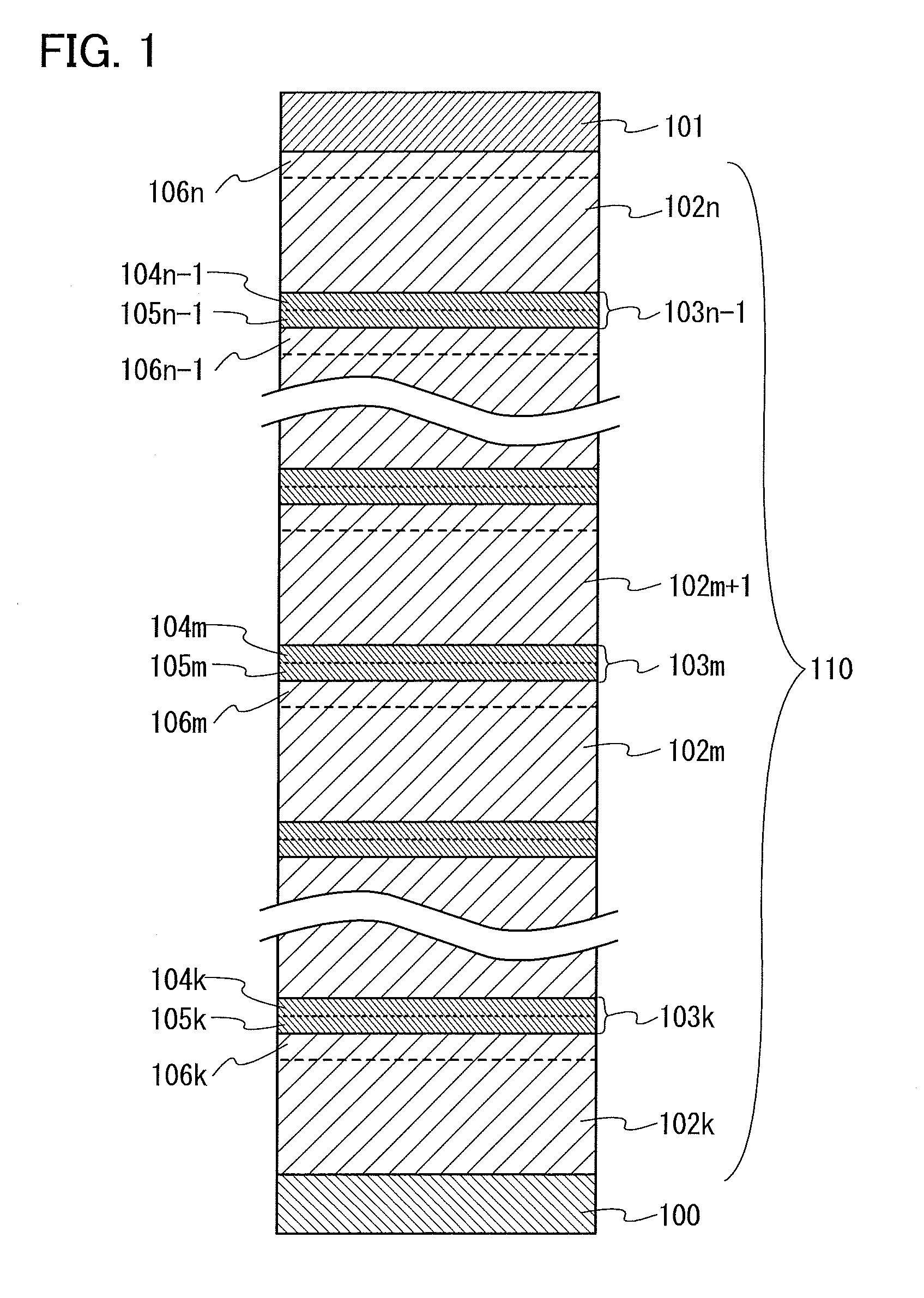
[0068]FIG. 1 is a conceptual diagram of a light-emitting element according to one embodiment of the present invention. The light-emitting element illustrated in FIG. 1 includes a plurality of (n) light-emitting units between a pair of electrodes (an anode 100 and a cathode 101). The light-emitting unit which is the closest to the anode 100 is a first light-emitting unit 102k, and the light-emitting unit which is the closest to the cathode 101 is an n-th light-emitting unit 102n.

[0069]The light-emitting element illustrated in FIG. 1 includes the light-emitting units (the first light-emitting unit 102k . . . an m-th light-emitting unit 102m . . . the n-th light-emitting unit 102n); charge generation layers (a first charge generation layer 103k . . . an m-th charge generation layer 103m . . . an (n−1)-th charge generation layer 103n−1); charge generation regions (a first charge generation region 104k . . . an m-th charge generation region 104m . . . an (n−1)-th charge ge...

embodiment 2

(Embodiment 2)

[0132]This embodiment shows a light-emitting device including the light-emitting element described in Embodiment 1.

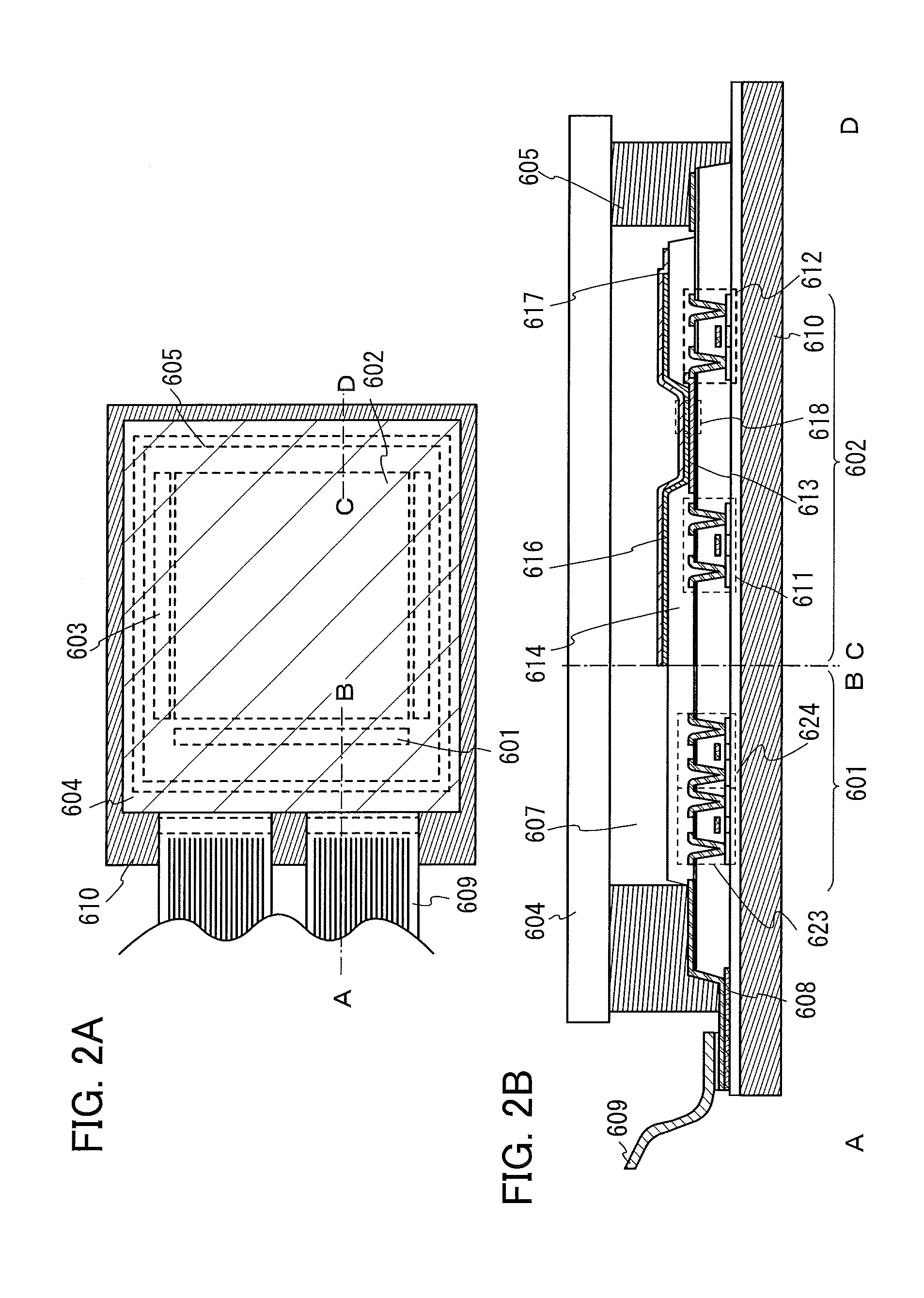
[0133]In this embodiment, the light-emitting device manufactured by using the light-emitting element described in Embodiment 1 will be described with reference to FIGS. 2A and 2B. FIG. 2A is a top view illustrating the light-emitting device, and FIG. 2B is a cross-sectional view of FIG. 2A taken along lines A-B and C-D. This light-emitting device includes a driver circuit portion (source line driver circuit) 601, a pixel portion 602, and a driver circuit portion (gate line driver circuit) 603, which are to control light emission of a light-emitting element and illustrated with dotted lines. A reference numeral 604 denotes a sealing substrate; 605 denotes a sealant; and a portion surrounded by the sealant 605 is a space 607.

[0134]A lead wiring 608 is a wiring for transmitting signals to be input to the source line driver circuit 601 and the gate line driver...

embodiment 3

(Embodiment 3)

[0157]In this embodiment, examples of an electronic device including the light-emitting element described in Embodiment 1 as part thereof will be described. The light-emitting element described in Embodiment 1 has high emission efficiency and consumes low power, and by using the light-emitting element, a display can provide high display quality. As a result, the electronic devices described in this embodiment can each have a display portion having high display quality and reduced power consumption.

[0158]Examples of the electronic device to which the above light-emitting element is applied include television devices (also referred to as TV or television receivers), monitors for computers and the like, cameras such as digital cameras and digital video cameras, digital photo frames, mobile phones (also referred to as cell phones or mobile phone devices), portable game machines, portable information terminals, audio playback devices, large game machines such as pachinko ma...


PUM


Abstract

A tandem light-emitting element in which generation of crosstalk can be suppressed even when the element is applied to a high-definition display is provided. In the tandem light-emitting element, a layer in contact the anode side of an intermediate layer contains 2,9-bis(naphthalen-2-yl)-4,7-diphenyl-1,10-phenanthroline (abbreviation: NBPhen).

Description

BACKGROUND OF THE INVENTION[0001]1. Field of the Invention[0002]The present invention relates to an object, a method, or a manufacturing method. In addition, the present invention relates to a process, a machine, manufacture, or a composition of matter. In particular, one embodiment of the present invention relates to a semiconductor device, a display device, a light-emitting device, a driving method thereof, or a manufacturing method thereof. In particular, one embodiment of the present invention relates to a light-emitting element which includes a light-emitting layer containing an organic compound between a pair of electrodes. Furthermore, the present invention relates to a light-emitting device including the light-emitting element and an electronic device including the light-emitting device.[0003]2. Description of the Related Art[0004]In recent years, mobile devices show remarkable development, and one can easily enjoy image works anytime and anywhere with a small image reproduc...

Claims


Application Information

Patent Timeline
Patent Type & Authority Patents(United States)
IPC IPC(8): H01L29/08H01L51/00H01L35/24H01L27/15H01L27/32H01L51/52H01L51/50H01L33/00H01L31/12H01L29/26
CPCH01L51/5012H01L27/3209H01L51/5278H01L27/322H01L51/0077H01L2251/53H10K59/32H10K59/38H10K85/30H10K50/19H10K50/11H10K50/805H10K59/35H10K85/342H10K85/371H10K85/615H10K85/622H10K85/626H10K85/633H10K85/6572H10K85/6576H10K2102/302
Inventor SUZUKI, TSUNENORIUESAKA, SHOGOYAMAOKA, RYOHEISEO, SATOSHI
Owner SEMICON ENERGY LAB CO LTD
Why Eureka
Try Eureka