Optical circuit

a technology of optical circuits and optical elements, applied in the field of optical circuits, can solve the problems of increasing construction costs, and achieve the effect of reducing construction costs and reducing the effect of

Active Publication Date: 2016-12-13
PHOTONICS ELECTRONICS TECH RES ASSOC
View PDF13 Cites 10 Cited by
  • Summary
  • Abstract
  • Description
  • Claims
  • Application Information

AI Technical Summary

Benefits of technology

[0026]According to the present invention, an optical circuit that reduces effect due to light reflected by optical components and that is constructed at low cost can be realized.

Problems solved by technology

However, each of these techniques merely prevents light reflected in a semiconductor laser module from returning to a semiconductor laser source.
However, since the optical isolator is an expensive optical component, this construction will increase the cost.

Method used


Image

  • Optical circuit
  • Optical circuit
  • Optical circuit

Examples


Embodiment Construction

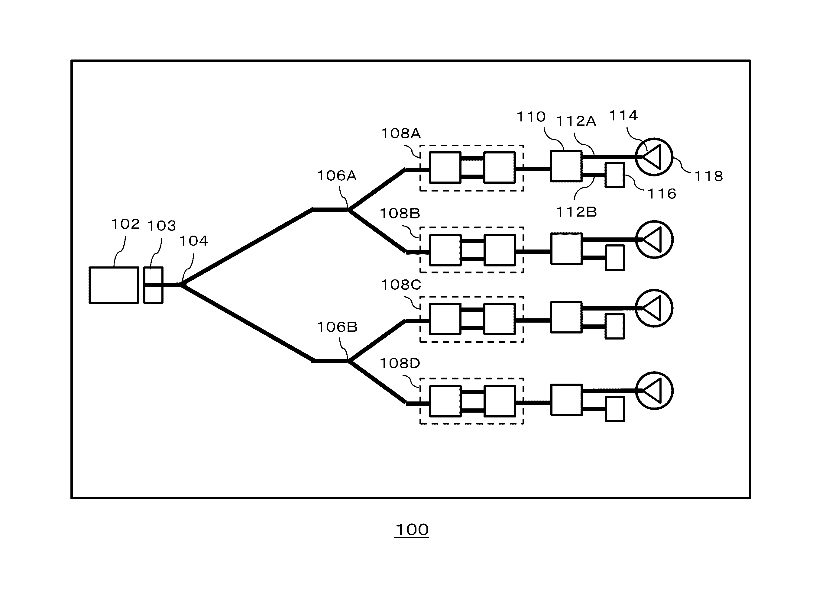
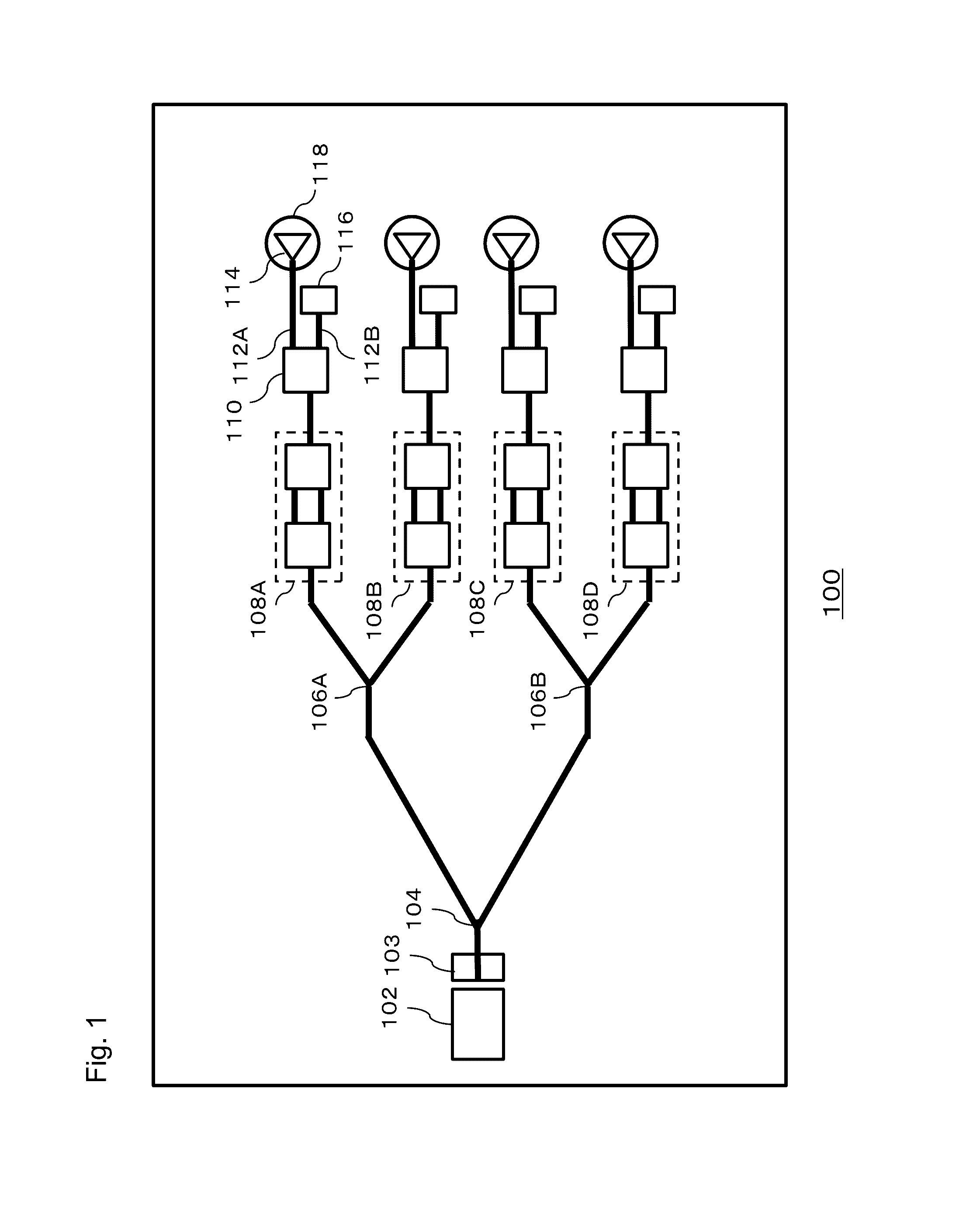
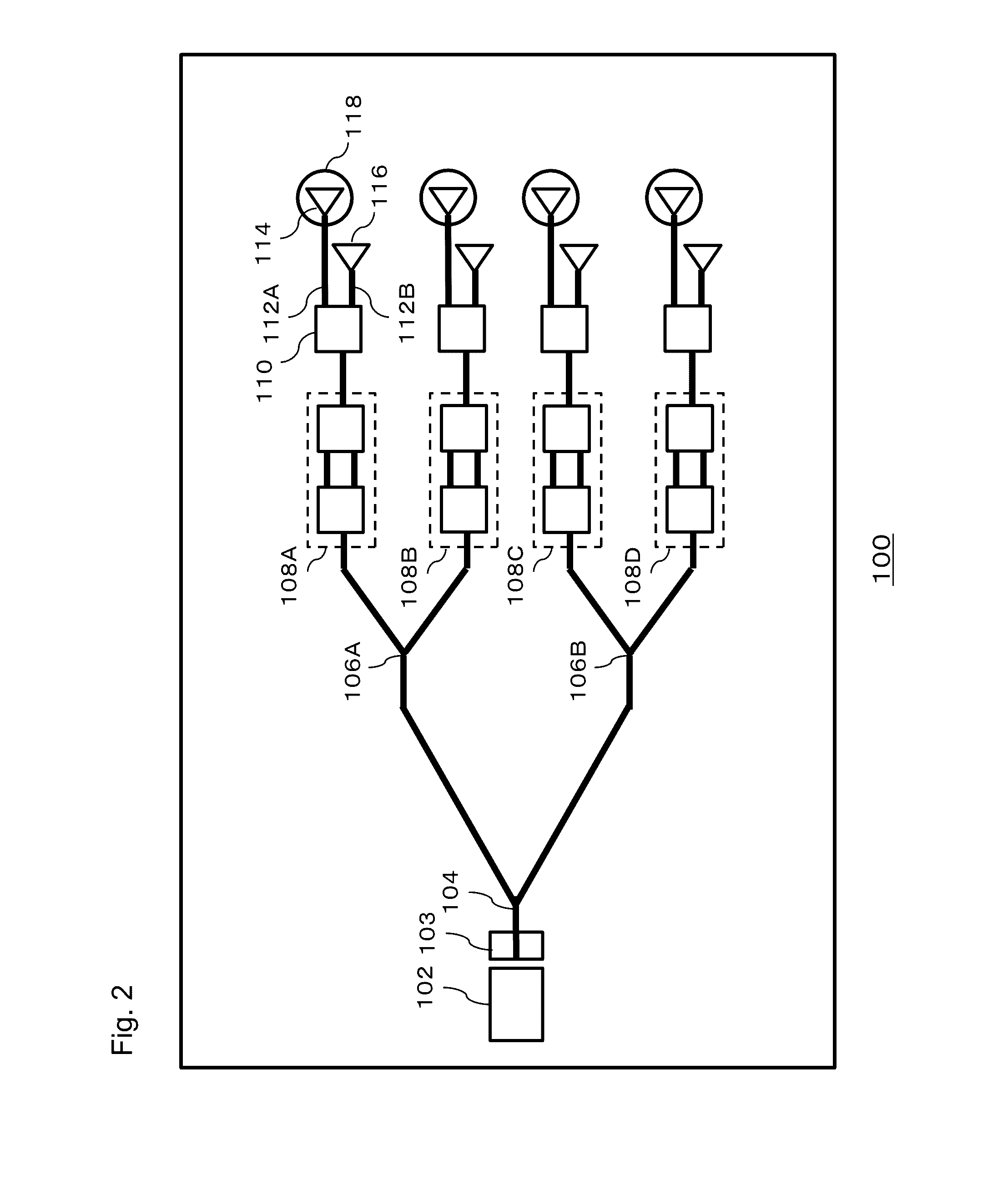
[0040]Embodiments of the present invention will be explained with reference to the drawings. FIG. 1 schematically shows an optical circuit 100 according to an embodiment of the present invention. The optical circuit 100 comprises a light source 102, optical branching parts 104, 106A, and 106B, and optical modulators 108A, 108B, 108C, and 108D. The light source 102 may comprise a semiconductor laser. The light emitted from the light source 102 is branched off to two waveguides at the optical branching part 104; further branched off to four waveguides at the optical branching parts 106A and 106B; and inputted to the optical modulators 108A, 108B, 108C, and 108D. Although the light from the optical source 102 is branched off to four optical waveguides in the present embodiment, the light from the optical source may be guided to one optical waveguide, or branched off to any number of optical waveguides. The optical modulators 108A, 108B, 108C, and 108D may be Mach-Zehnder interferometer...


PUM

PropertyMeasurementUnit
distanceaaaaaaaaaa
core diameteraaaaaaaaaa
wavelengthaaaaaaaaaa

Abstract

An optical circuit, wherein the effects of reflected light generated by an optical component are reduced. The optical circuit (100) is provided with an optical branching (110) for branching light, an optical coupler (114) for coupling a first portion of branched light to an optical waveguide (118) for transmission, and an optical reflecting unit (116) for reflecting a second portion of the branched light, the phase difference between the reflected light from the optical coupler (114) and the reflected light from the optical reflecting unit (116) being (2m−1)π (where m is an integer) on an input side of the optical branching (110).

Description

TECHNICAL FIELD[0001]The present invention relates to an optical circuit, and in particular, to an optical circuit that prevents deterioration of performance due to reflected light.BACKGROUND ART[0002]In an optical communication system, it is required to stabilize the operation of a semiconductor laser used as a light source.[0003]To do so, in Patent-related Document 1, it is suggested to prevent light reflected by a wavelength filter from returning to a semiconductor laser, when monitoring oscillation wavelength of the semiconductor laser by using, via the wavelength filter, an optical detector.[0004]In Patent-related Document 2, it is suggested to guide the light reflected by an optical resonator placed within an external modulator, toward a direction different from a direction of a semiconductor laser.[0005]However, each of these techniques merely prevents light reflected in a semiconductor laser module from returning to a semiconductor laser source. Thus, even if an optical comm...

Claims


Application Information

Patent Timeline
Patent Type & Authority Patents(United States)
IPC IPC(8): G02F1/035G02B6/30G02B6/34G02B6/42G02B6/125G02B6/124G02B6/12G02B6/28
CPCG02B6/4207G02B6/12004G02B6/125G02B6/305G02B6/34G02B6/28G02B2006/12123G02B2006/12142H01S5/0064H01S5/0085
Inventor YASHIKI, KENICHIROTOKUSHIMA, MASATOSHI
Owner PHOTONICS ELECTRONICS TECH RES ASSOC
Why Eureka
Try Eureka