Nonvolatile logic gate device

a logic gate and non-volatile technology, applied in the field of non-volatile logic gate devices, can solve the problems of difficult enhancement or improvement of logic gate error tolerance, inability to readily perform error detection or error correction of memory data stored in such a non-volatile logic gate, etc., to achieve increase of circuit area, increase of electric power consumption, and increase of error tolerance

Active Publication Date: 2017-01-03
NEC CORP +1
View PDF9 Cites 4 Cited by
  • Summary
  • Abstract
  • Description
  • Claims
  • Application Information

AI Technical Summary

Benefits of technology

[0029]According to the present invention, there can be provided a nonvolatile logic gate using resistance random access elements that have an enhanced error tolerance while an increase of the circuit area and an increase of the electric power consumption are prevented, and an integrated circuit using such a nonvolatile logic gate.

Problems solved by technology

First, an error detection or an error correction of memory data stored in such a nonvolatile logic gate cannot readily be performed as it is.
Thus, it is difficult to enhance or improve an error tolerance of the logic gate.
Examples of errors in memory data include a writing soft error caused to occur with a very low probability such that data different than intended are written and a soft error caused such that stored data are inversed for some reasons.

Method used


Image

  • Nonvolatile logic gate device
  • Nonvolatile logic gate device
  • Nonvolatile logic gate device

Examples


first embodiment

[0051]FIG. 4 is a circuit diagram of a nonvolatile logic gate 1 having an enhanced error tolerance according to a first embodiment, as compared to existing nonvolatile logic gates.

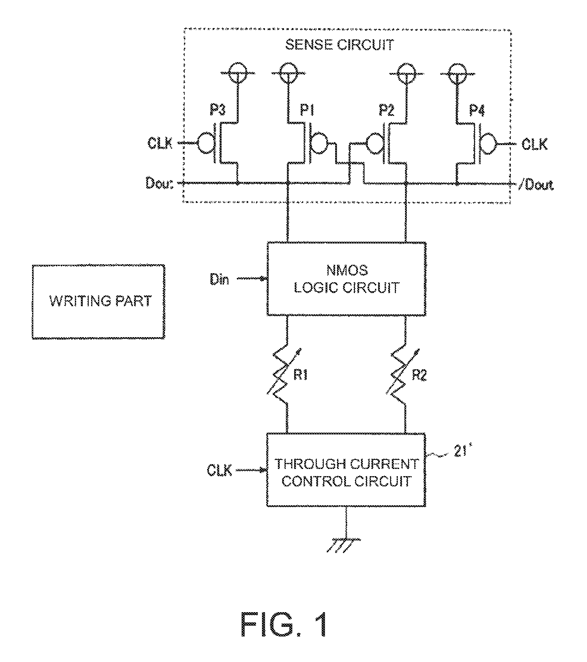
[0052]As shown in FIG. 4, the nonvolatile logic gate 1 is part of an integrated circuit in which a memory element and a logic element are integrated with each other and includes a nonvolatile resistive network aggregation 11, a writing part 21, an NMOS logic circuit 31, a through current control circuit 41, and a sense circuit 51.

[0053]The NMOS logic circuit 31, the through current control circuit 41, and the sense circuit 51 of the present embodiment can employ the aforementioned circuit configuration described in Patent Literature 1.

[0054]The nonvolatile resistive network aggregation 11 includes a first nonvolatile resistive network having three nonvolatile resistive elements R1, R2, and R3 connected in series and a second nonvolatile resistive network having a value Rref, which is a reference resistance...

second embodiment

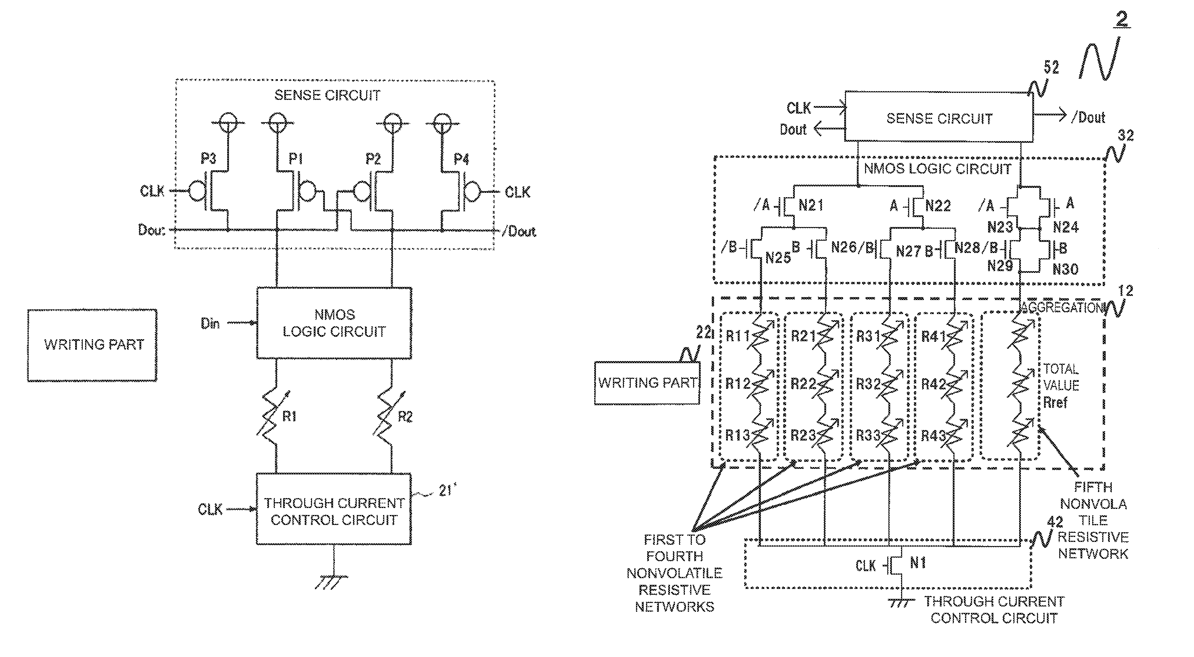
[0088]FIG. 7 is a circuit diagram of a nonvolatile resistive network aggregation 12 according to a second embodiment and a nonvolatile logic gate 2 having an enhanced error tolerance with use of the nonvolatile resistive network aggregation 12.

[0089]In the present embodiment, the nonvolatile resistive network aggregation 12 includes a plurality of nonvolatile resistive networks. The nonvolatile logic gate 2 of the present embodiment serves as a 2-input lookup table. The nonvolatile resistive network aggregation 12 of the present embodiment is formed by a first nonvolatile resistive network, which includes three nonvolatile resistive elements R11, R12, and R13, a second nonvolatile resistive network, which includes three nonvolatile resistive elements R21, R22, and R23, a third nonvolatile resistive network, which includes three nonvolatile resistive elements R31, R32, and R33, and a fourth nonvolatile resistive network, which includes three nonvolatile resistive elements R41, R42, a...

third embodiment

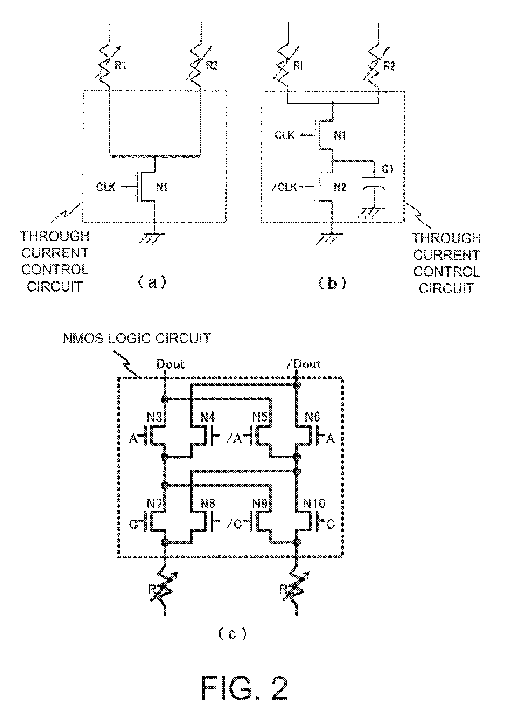
[0096]FIG. 8 is a circuit diagram of a nonvolatile resistive network aggregation 13 according to a third embodiment and a nonvolatile logic gate 3 having an enhanced error tolerance with use of the nonvolatile resistive network aggregation 12. The nonvolatile resistive network aggregation 13 of the present embodiment includes a first nonvolatile resistive network, which includes three nonvolatile resistive elements R1, R2, and R3. A second nonvolatile resistive network is configured to have a resistance value Rref.

[0097]The nonvolatile resistive elements R1, R2, and R3 are connected to each other in series. An end of the nonvolatile resistive elements R1, R2, and R3 is connected to an input terminal of an inverter circuit, and the other end of the nonvolatile resistive elements R1, R2, and R3 is grounded to a Gnd voltage. The second nonvolatile resistive network is configured to have a resistance value Rref. An end of the second nonvolatile resistive network is connected to the inpu...


PUM


Abstract

A nonvolatile logic gate device is configured to include a resistive network of a memory structure in which at least three nonvolatile resistive elements are connected, a reference resistive network as a reference resistance providing a tolerance of the memory structure to a resistance value of the resistive network of the memory structure, a writing part operable to selectively write or rewrite a value of each of the nonvolatile resistive elements in the resistive network into a maximum or a minimum corresponding to a logical value to be read when data are stored into the resistive network, and a logic circuit structure operable to use, as a logical value of the memory structure, a value obtained by comparison between the resistance value of the resistive network and the resistance value of the reference resistive network.

Description

CROSS REFERENCE TO RELATED APPLICATIONS[0001]This application is a National Stage of International Application No. PCT / JP2013 / 064138 filed May 15, 2013, claiming priority based on Japanese Patent Application No. 2012-132412, filed Jun. 11, 2012, the contents of all of which are incorporated herein by reference in their entirety.TECHNICAL FIELD[0002]The present invention relates to a nonvolatile logic gate device which has a nonvolatile data memory structure by the use of resistance random access elements, and more particularly to a nonvolatile logic gate device which has an error tolerance against data writing and an integrated circuit which has such a nonvolatile logic gate device.BACKGROUND ART[0003]In recent years, an increase of electric power consumption caused by leakage currents of transistors has been problematic as a degree of integration of semiconductors increases. An arrangement in which a memory element and a logic element have been separated from each other results in ...

Claims


Application Information

Patent Timeline
Patent Type & Authority Patents(United States)
IPC IPC(8): G11C11/00G11C13/00H03K3/356G11C11/16H03K19/18
CPCG11C11/1675G11C11/161G11C11/1673G11C13/0002G11C13/003G11C13/004G11C13/0069H03K3/356121H03K19/18G11C2013/0054G11C2213/75G11C2213/78G11C2213/79
Inventor NEBASHI, RYUSUKESAKIMURA, NOBORUTSUJI, YUKIHIDETADA, AYUKASUGIBAYASHI, TADAHIKOHANYU, TAKAHIROENDOH, TETSUOOHNO, HIDEO
Owner NEC CORP
Why Eureka
Try Eureka