Fiber coupler for silicon photonics

a technology of silicon photonics and couplers, applied in the field of fiber couplers and methods for coupling fibers to silicon waveguides, can solve the problems of serial link performance being limited by the electrical bandwidth of channels and electronic components, affecting the performance of serial links, and requiring a huge amount of bandwidth for transferring photo, video, music and other multimedia files. , to achieve the effect of reducing power loss and high bandwidth

Active Publication Date: 2017-01-17
MARVELL ASIA PTE LTD
View PDF32 Cites 22 Cited by
  • Summary
  • Abstract
  • Description
  • Claims
  • Application Information

AI Technical Summary

Benefits of technology

[0005]The present invention relates to silicon photonic devices and methods. Various embodiments of the present invention provide a fiber coupling device for coupling a single-mode optical fiber to a buried silicon waveguide. More specifically, multiple embodiments provide methods for forming coupling structures to adapt the optical mode such that the light from the silicon core of the buried waveguide can be coupled into the fiber core with substantially minimized power loss. In certain embodiments, the invention is applied for high bandwidth optical communication, though other applications are possible.

Problems solved by technology

But Internet and mobile applications continuously demand a huge amount of bandwidth for transferring photo, video, music, and other multimedia files.
Serial link performance is limited by the channel electrical bandwidth and the electronic components.
Stacking chips into so-called 3-D ICs promises a one-time boost in their capabilities, but it's very expensive.

Method used


Image

  • Fiber coupler for silicon photonics
  • Fiber coupler for silicon photonics
  • Fiber coupler for silicon photonics

Examples


Embodiment Construction

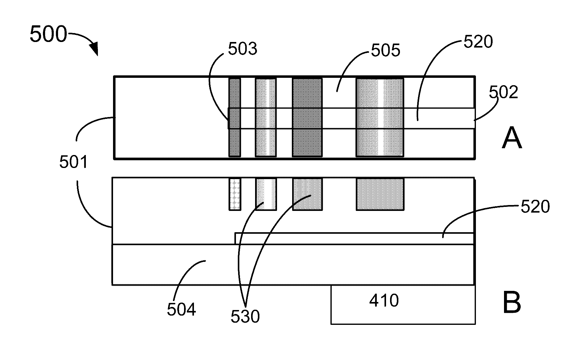
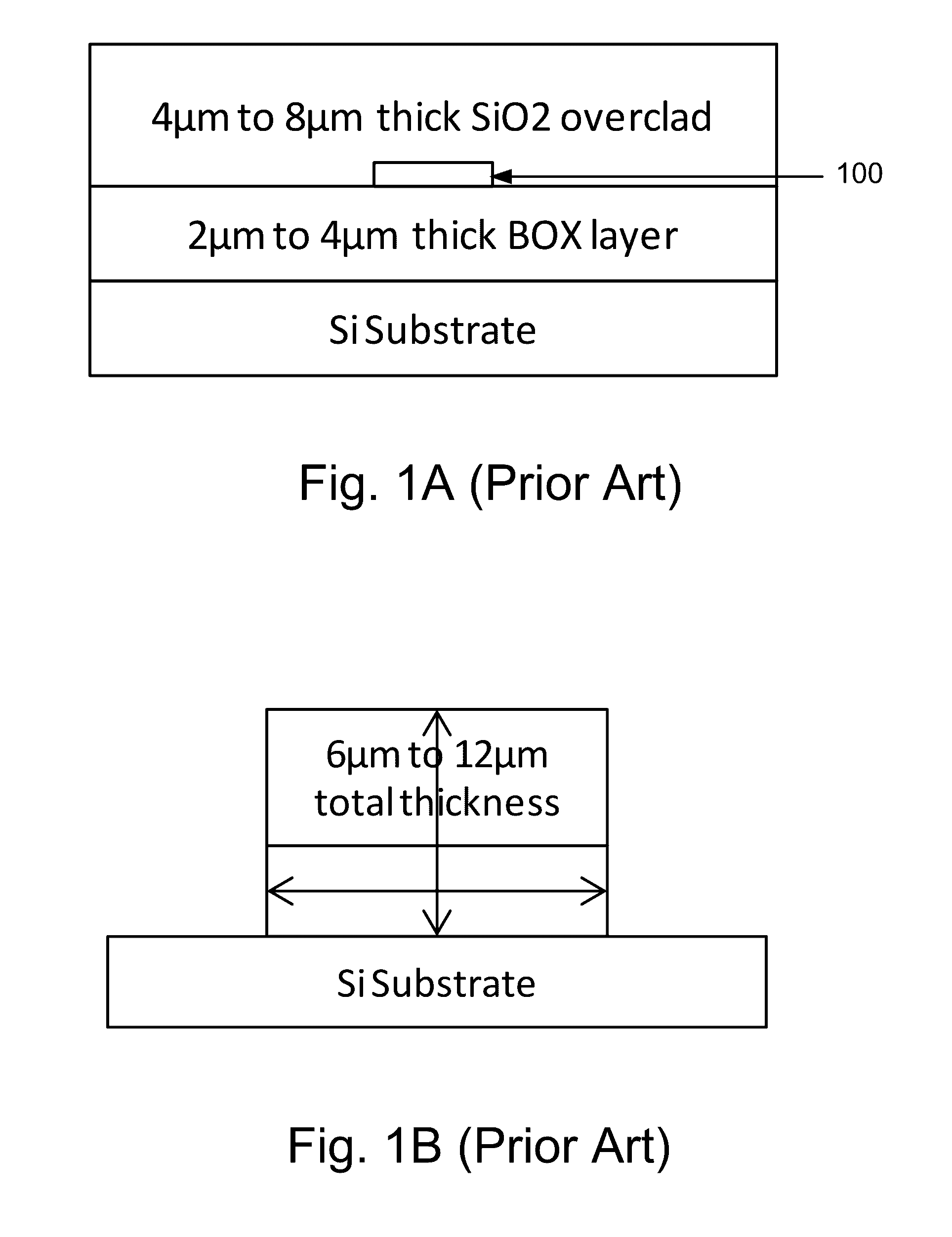
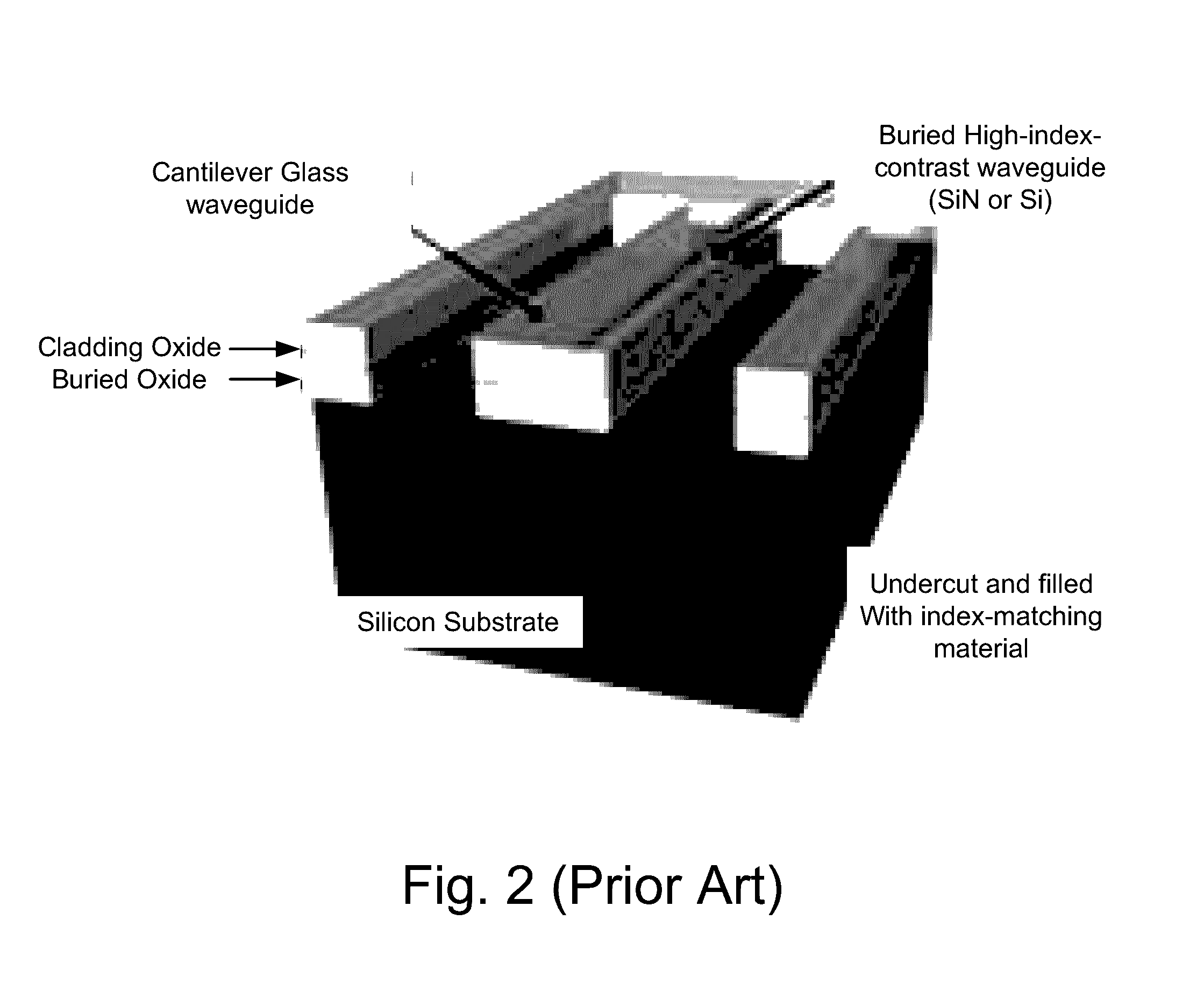
[0027]The present invention relates to silicon photonic devices and methods. Various embodiments of the present invention provide a fiber coupling device for coupling a single-mode optical fiber to a buried silicon waveguide. More specifically, multiple embodiments provide methods for forming coupling structures to adiabatically adapt the mode such that the light from the silicon core of the buried waveguide can be coupled to the fiber with reduced power loss. In certain embodiments, the invention is applied for high bandwidth optical communication, though other applications are possible.

[0028]The following description is presented to enable one of ordinary skill in the art to make and use the invention and to incorporate it in the context of particular applications. Various modifications, as well as a variety of uses in different applications will be readily apparent to those skilled in the art, and the general principles defined herein may be applied to a wide range of embodiments...


PUM


Abstract

An apparatus for converting fiber mode to waveguide mode. The apparatus includes a silicon substrate member and a dielectric member having an elongated body. Part of the elongated body from a back end overlies the silicon substrate member and remaining part of the elongated body up to a front end is separated from the silicon substrate member by a second dielectric material at an under region. The apparatus also includes a waveguide including a segment from the back end to a tail end formed on the dielectric member at least partially overlying the remaining part of the elongated body. The segment is buried in a cladding overlying entirely the dielectric member. The cladding has a refractive index that is less than the waveguide but includes an index-graded section with decreasing index that is formed at least over the segment from the tail end toward the back end.

Description

CROSS-REFERENCE TO RELATED APPLICATIONS[0001]N / ABACKGROUND OF THE INVENTION[0002]The present invention relates to silicon photonic devices and methods. More particularly, the present invention provides improved fiber couplers and methods for coupling fiber to silicon waveguide with enhanced coupling efficiency.[0003]Over the last few decades, the use of communication networks exploded. In the early days Internet, popular applications were limited to emails, bulletin board, and mostly informational and text-based web page surfing, and the amount of data transferred was usually relatively small. Today, Internet and mobile applications demand a huge amount of bandwidth for transferring photo, video, music, and other multimedia files. For example, a social network like Facebook processes more than 500 TB of data daily. With such high demands on data and data transfer, existing data communication systems need to be improved to address these needs.[0004]Over the past, the conventional fib...

Claims


Application Information

Patent Timeline
Patent Type & Authority Patents(United States)
IPC IPC(8): G02B6/00G02B6/30G02B6/122G02B6/245G02B6/26
CPCG02B6/26G02B6/245G02B6/305G02B6/1228G02B6/136G02B2006/12061
Inventor KATO, MASAKINAGARAJAN, RADHAKRISHNAN L.
Owner MARVELL ASIA PTE LTD
Why Eureka
Try Eureka