Light emitting diode load board and manufacturing process thereof

a technology of light-emitting diodes and load-bearing boards, which is applied in the direction of resist details, printed circuit aspects, printed element electric connection formation, etc., can solve the problems of difficulty in assembling process, increase temperature, and decrease the yield rate of load-bearing boards, so as to enhance the efficiency of aligning and connecting, and enhance the thermal conductivity of led load-bearing boards

Inactive Publication Date: 2017-01-31
TM TECHNOLOGY INC
View PDF5 Cites 1 Cited by
  • Summary
  • Abstract
  • Description
  • Claims
  • Application Information

AI Technical Summary

Benefits of technology

[0012]As described above, the structure of the LED load board in the disclosure may not only avoid the interconnection between different conductive layers but also has conductive pillars at the interface with LEDs, and these conductive pillars are helpful to the aligning connection with LEDs. Moreover, in an embodiment polysilicon is used to form one of the constitution layers of the LED load board, so the thermal conductivity of the LED load board may be enhanced. Therefore, the LED load board and the manufacturing method thereof may enhance the efficiency of aligning and connecting the LED load board to LEDs and also enhance the thermal conductivity of the LED load board.

Problems solved by technology

In practice, the luminous efficiency of a LED rapidly drops under the influence of a high temperature environment, so the LED wastes more power and also produces more heat, resulting in the increase of temperature.
This will bring in a difficulty in the assembling process and also decrease the yield rate of the manufacturing of load boards.

Method used


Image

  • Light emitting diode load board and manufacturing process thereof
  • Light emitting diode load board and manufacturing process thereof
  • Light emitting diode load board and manufacturing process thereof

Examples


Embodiment Construction

[0025]In the following detailed description, for purposes of explanation, numerous specific details are set forth in order to provide a thorough understanding of the disclosed embodiments. It will be apparent, however, that one or more embodiments may be practiced without these specific details. In other instances, well-known structures and devices are schematically shown in order to simplify the drawings.

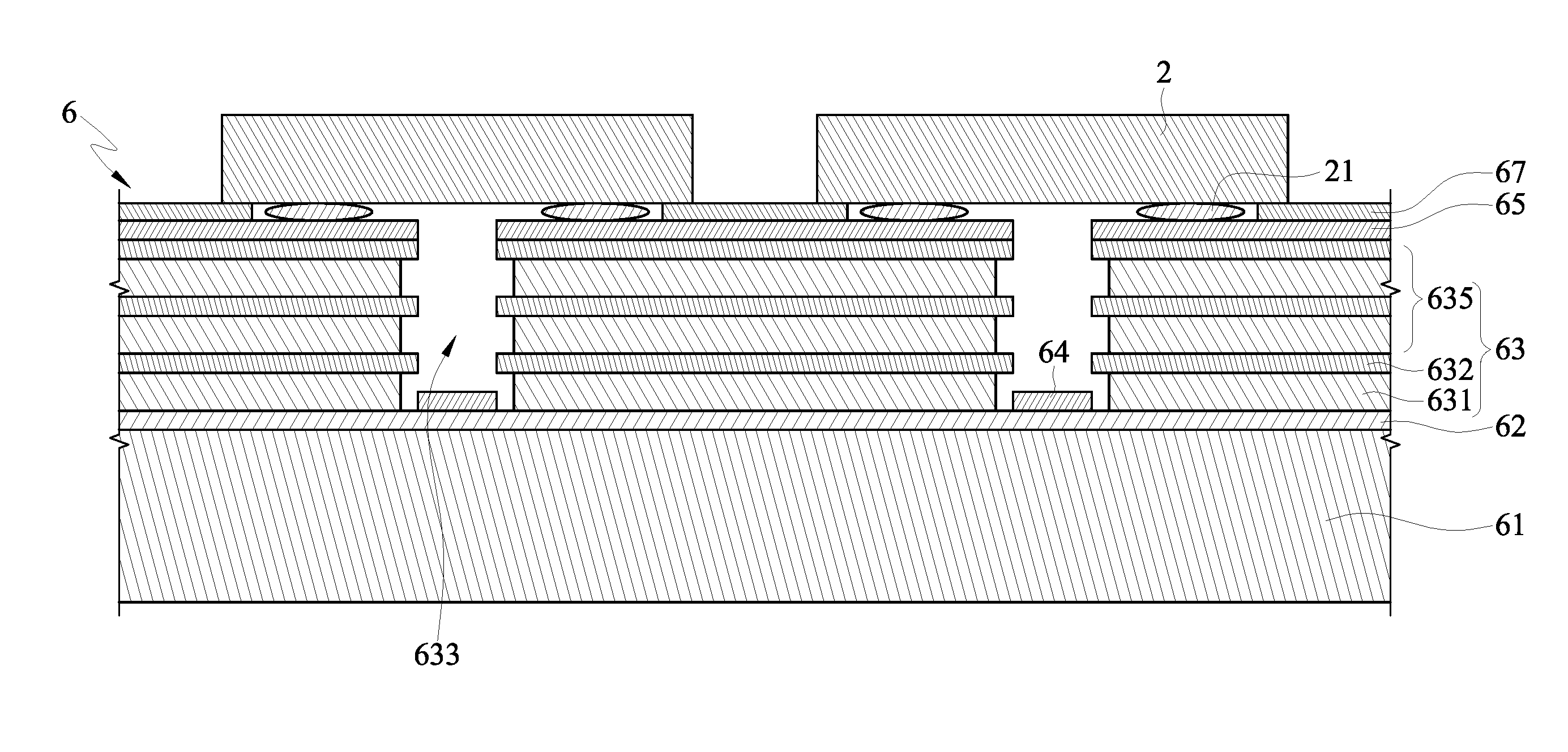
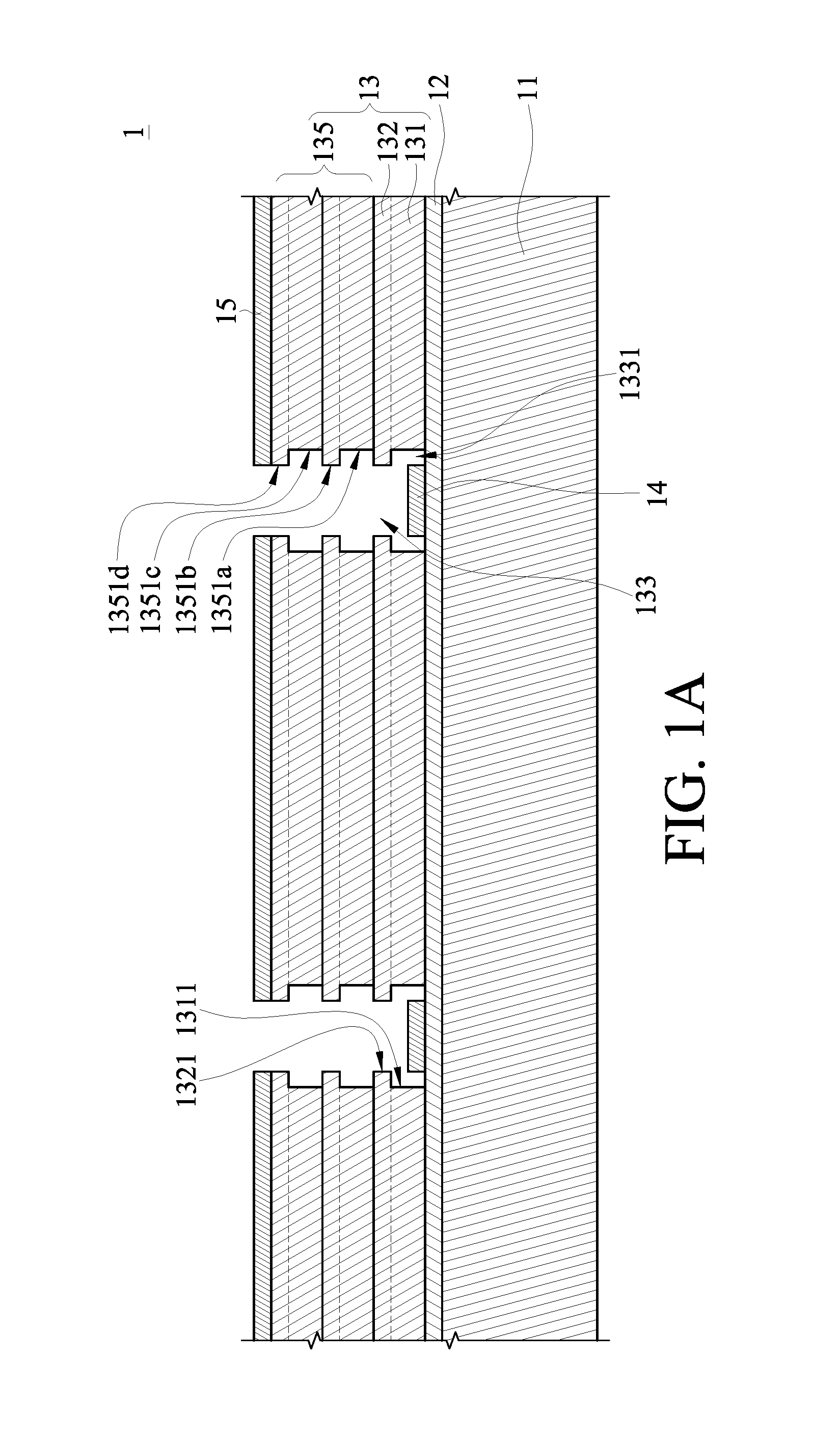
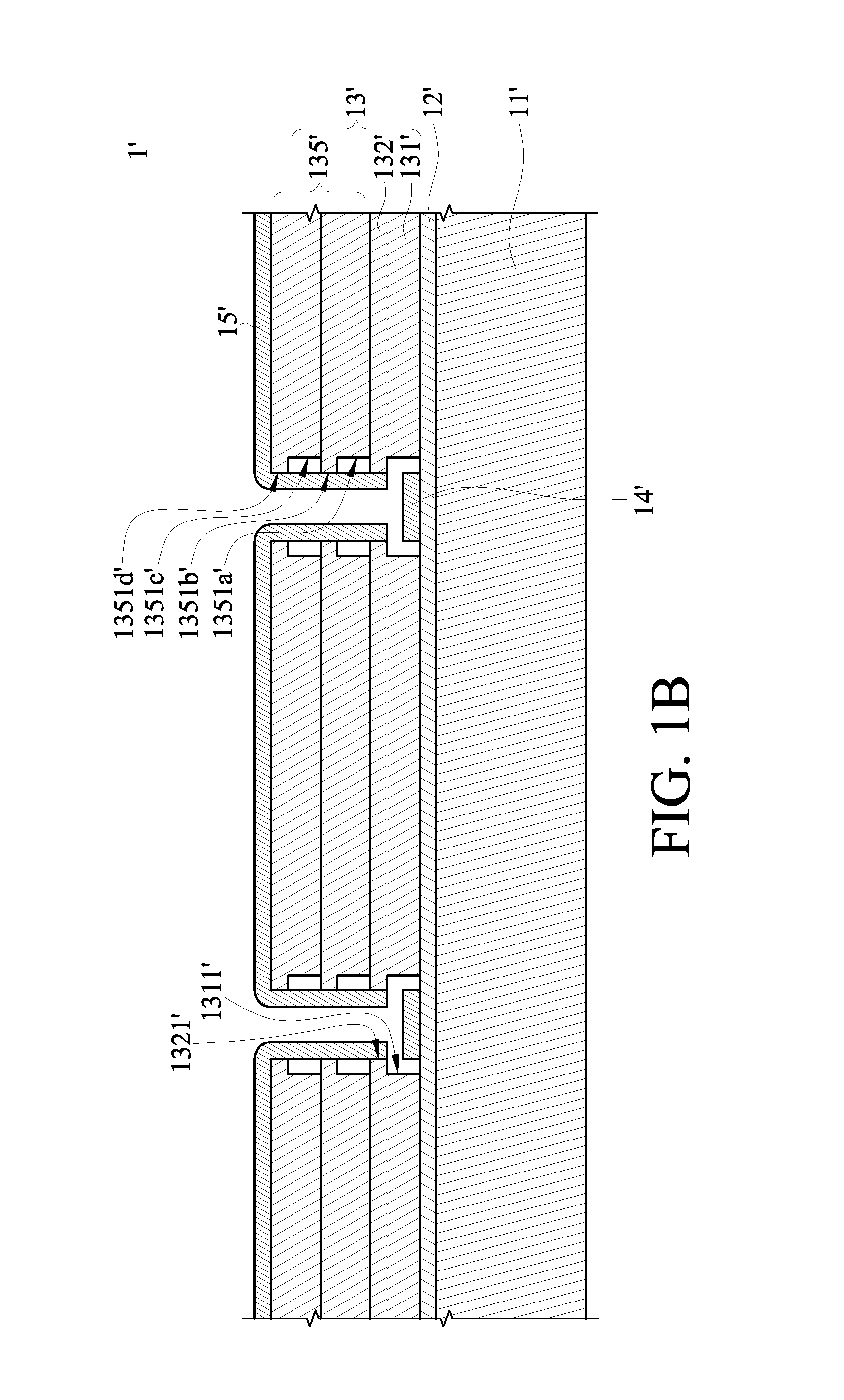
[0026]Please refer to FIG. 1A. FIG. 1A is a schematic structure diagram of a LED load board in an embodiment. A LED load board 1 includes a substrate 11, a first dielectric layer 12, a second dielectric layer 13, a first conductive pad 14 and a second conductive pad 15. The second dielectric layer 13 includes a first structure portion 131, a second structure portion 132 and a third structure portion 135. The first structure portion 131 includes a first sidewall 1311, the second structure portion 132 includes a second sidewall 1321, and the third structure portion 135 is constructed...


PUM


Abstract

A light emitting diode load board includes a substrate, a first dielectric layer, a second dielectric layer and a first conductive pad and a second conductive pad. The second dielectric layer includes a first structure part, a second structure part and a third structure part. The first dielectric layer is disposed on the substrate. The first structure part is disposed on the first dielectric layer and has a first sidewall. The second structure part is disposed on the first structure part and has a second sidewall. The third structure part is disposed on the second structure part and has N sidewalls. The second sidewall is more prominent than the first sidewall. The first sidewall, the second sidewall and the N sidewalls define the first etched part, and the part of the first dielectric layer is exposed from the first etched part. The first conductive pad is disposed in the first etched part. The second conductive is disposed on the second dielectric layer, covers part of the second dielectric and exposes the open of the first etched part.

Description

CROSS-REFERENCE TO RELATED APPLICATIONS[0001]This non-provisional application claims priority under 35 U.S.C. §119(a) on Patent Application No(s). 62 / 148,722 filed in the United States on Apr. 16, 2015, the entire contents of which are hereby incorporated by reference.BACKGROUND[0002]Technical Field[0003]The disclosure relates to a light emitting diode (LED) load board and a manufacturing method thereof, more particularly to a LED load board with an alignment structure and a manufacturing method thereof.[0004]Related Art[0005]Generally, when LEDs are powered to emit light, the supplied power is partly used to emit light and partly converted into thermal energy. In practice, the luminous efficiency of a LED rapidly drops under the influence of a high temperature environment, so the LED wastes more power and also produces more heat, resulting in the increase of temperature. The LED then falls into a vicious spiral. Therefore, it would be better to load LEDs on a load board with a bett...

Claims


Application Information

Patent Timeline
Patent Type & Authority Patents(United States)
IPC IPC(8): H05K1/11H05K1/09H05K1/02H05K3/46H05K3/40H05K3/00
CPCH05K1/0298H05K1/09H05K1/111H05K3/0017H05K3/4007H05K3/4644H05K2201/09036H05K2201/10106H05K2201/10242H05K2203/0562H01L33/005H01L33/62H01L33/641H01L2933/0066H01L2933/0075H01L33/64H01L2224/16225H05K2201/0187H05K2201/0195
Inventor WU, BENSU, WEN-DOE
Owner TM TECHNOLOGY INC
Why Eureka
Try Eureka