Heterostructure field-effect transistor

a technology of field effect transistor and structure, applied in the direction of basic electric elements, electrical apparatus, semiconductor devices, etc., can solve the problem that the performance of components has reached a performance bottleneck in energy conversion efficiency

Active Publication Date: 2017-02-21
EPISTAR CORP
View PDF18 Cites 11 Cited by
  • Summary
  • Abstract
  • Description
  • Claims
  • Application Information

AI Technical Summary

Benefits of technology

[0007]An object of the present invention is to provide a HFET using a p-type group IIIA-VA ...

Problems solved by technology

Most conventional power components are based on Si-based materials, because Si material is relatively inexpensive and is considered a well-understood material, but...

Method used


Image

  • Heterostructure field-effect transistor
  • Heterostructure field-effect transistor
  • Heterostructure field-effect transistor

Examples


Embodiment Construction

[0030]The present invention will now be described more specifically with reference to the following embodiments. It is to be noted that the following descriptions of the embodiments of this invention are presented herein for purpose of illustration and description only. It is not intended to be exhaustive or to be limited to the precise form disclosed.

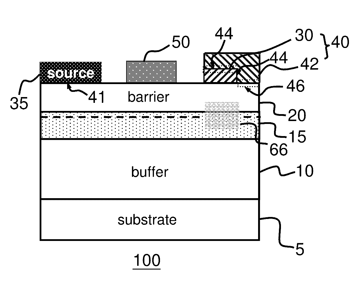
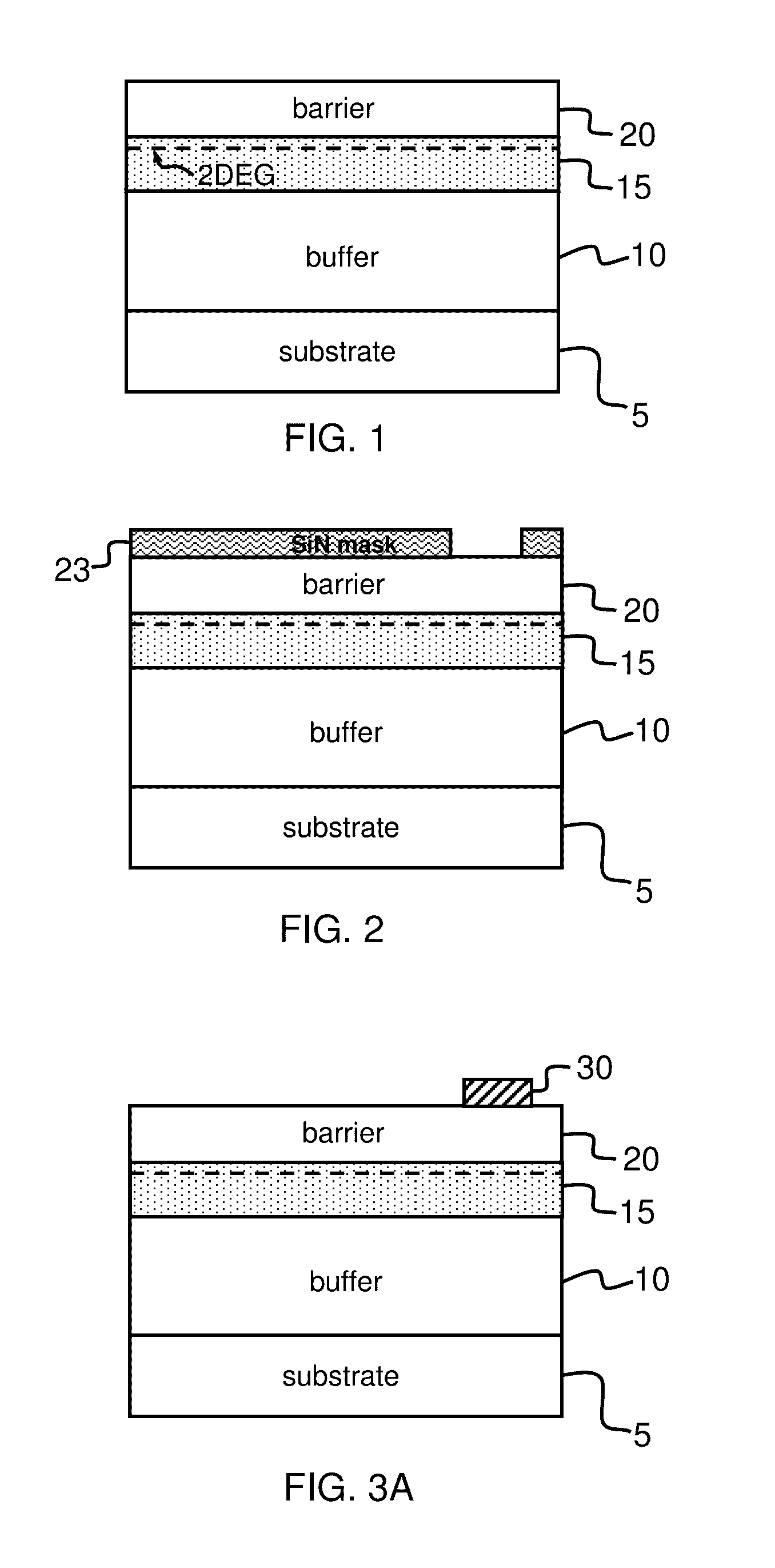
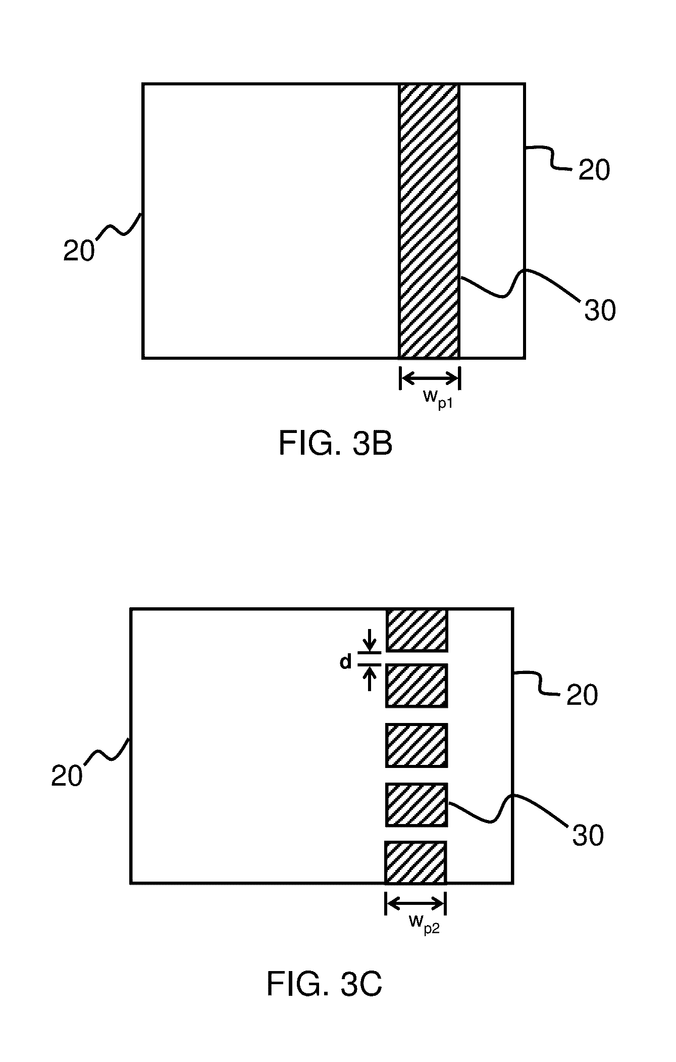
[0031]Referring to FIGS. 1-5, a first method for fabricating a heterostructure field effect transistor (HFET) device 100 according to an embodiment of present invention includes the following steps: in a first step, a buffer layer 10, a channel layer 15 including a first group IIIA-VA semiconductor material, and an barrier layer 20 including a first group IIIA-VA semiconductor material are respectively epitaxially grown by metal organic chemical-vapor deposition (MOCVD), hydride vapor phase epitaxy (HVPE), liquid phase epitaxy (LPE), and so forth on a substrate 5 in sequential order as shown in FIG. 1. A two-dimensional electron gas (2...


PUM


Abstract

Heterostructure field-effect transistor (HFET) having a channel layer, a barrier layer disposed on the channel layer, and a gate, source and drain electrodes disposed on the barrier layer, respectively, and corresponding fabrication methods are disclosed. The drain electrode includes a p-type semiconductor patterned structure and a raised drain section, the drain electrode includes a Schottky contact and an ohmic contact, the Schottky contact is formed between a top surface together with a side surface of p-type semiconductor patterned structure and a bottom surface together with a side surface of raised drain section, the ohmic contact is formed between another surface of raised drain section and barrier layer, the raised drain section partially surrounding the p-type semiconductor patterned structure, and a bandgap of the channel layer is less than a bandgap of the barrier layer.

Description

BACKGROUND OF THE INVENTION[0001](a) Field of the Invention[0002]The present invention is related to a heterostructure field effect transistor (HFET), and more particularly, to a group IIIA-VA HFET and method of fabricating the same.[0003](b) Description of the Prior Art[0004]Today Schottky barrier diodes are used in many power switching applications such as switch mode power supplies (SMPS), converters, and inverters. Engineers and scientists have used heterostructure FET (HFET) or high-electron-mobility transistor (HEMT) to create Schottky barrier diodes. A heterostructure FET (HFET) or a high-electron-mobility transistor (HEMT) is a field-effect transistor (FET) incorporating a junction between two materials with different band gaps (i.e. a heterojunction) as the channel instead of a doped region as is the case generally for MOSFET. Most conventional power components are based on Si-based materials, because Si material is relatively inexpensive and is considered a well-understood...

Claims


Application Information

Patent Timeline
IPC IPC(8): H01L21/00H01L29/778H01L29/417H01L29/66H01L21/306H01L21/02H01L21/283H01L21/308H01L29/20H01L21/311H01L29/205H01L21/31
CPCH01L29/205H01L29/7787H01L29/41783H01L29/66462H01L21/31H01L21/0262H01L21/283H01L21/308H01L29/2003H01L21/02458H01L21/0254H01L21/31116H01L21/30612H01L29/41725H01L29/7786H01L29/0619H01L21/28581H01L21/28593H01L29/41758H01L29/475
Inventor YANG, YA-YULIN, PING-HAO
Owner EPISTAR CORP
Why Eureka
Try Eureka