Semiconductor integrated circuit structure including dielectric having negative thermal expansion

Active Publication Date: 2017-04-25
UNITED MICROELECTRONICS CORP
View PDF5 Cites 2 Cited by
  • Summary
  • Abstract
  • Description
  • Claims
  • Application Information

AI Technical Summary

Benefits of technology

[0008]According to the semiconductor IC structure and the method for forming the same, the second dielectric layer including the CTE smaller than zero is formed between the first conductive layer and the second conductive layer. In other words, there is provided a negative thermal expansion (NTE) material sandwiched between the first conductive layer and t

Problems solved by technology

However, it is found dielectric layers suffer cracking more than conductive layers.
And crack

Method used


Image

  • Semiconductor integrated circuit structure including dielectric having negative thermal expansion
  • Semiconductor integrated circuit structure including dielectric having negative thermal expansion
  • Semiconductor integrated circuit structure including dielectric having negative thermal expansion

Examples


Example

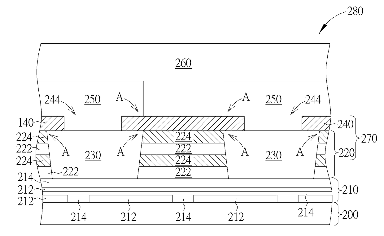
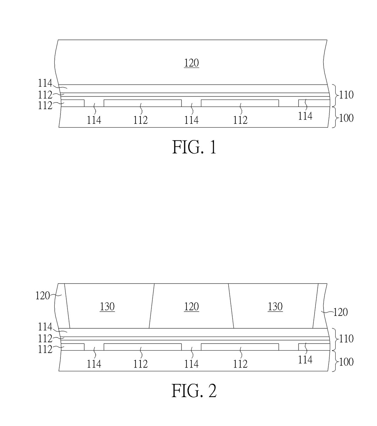
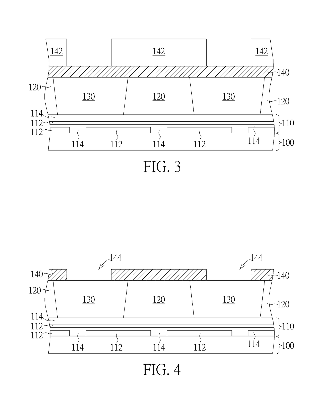
[0020]Please refer to FIGS. 1-6, which are drawings illustrating a method for forming a semiconductor IC structure provided by a first preferred embodiment of the present invention. As shown in FIG. 1, a semiconductor substrate 100 is provided, and IC(s) including a plurality of active and passive devices (not shown) can be fabricated in the semiconductor substrate 100 by front-end-of-line (hereinafter abbreviated as FEOL) process. The semiconductor substrate 100 is typically a wafer comprising multiple dies and each die includes a piece of a semiconductor material including, for example but not limited to, silicon (Si), silicon germanium (SiGe), a silicon-on-insulator (SOI) layer, and other like silicon-containing semiconductor materials. Device designs for the above mentioned active / passive devices and the details of the FEOL process are familiar to a person having ordinary skill in the art, therefore those details are all omitted in the interest of brevity.

[0021]Please refer to F...


PUM


Abstract

A semiconductor IC structure includes a semiconductor substrate, a multi-layered dielectric structure disposed on the semiconductor substrate, a first conductive layer disposed in the multi-layered dielectric structure, and a second conductive layer disposed on the multi-layered dielectric structure. The multi-layered dielectric structure further includes a first dielectric layer disposed on the semiconductor substrate, and a second dielectric layer disposed on the first dielectric layer. A coefficient of thermal expansion (CTE) of the first dielectric layer is larger than zero, and a CTE of the second dielectric layer is smaller than zero.

Description

BACKGROUND OF THE INVENTION[0001]1. Field of the Invention[0002]The invention relates to a semiconductor integrated circuit (hereinafter abbreviated as IC) structure and a method for forming the same, and more particularly, to a semiconductor IC structure including negative thermal expansion (hereinafter abbreviated as NTE) material and a method for forming the same.[0003]2. Description of the Prior Art[0004]Semiconductor IC structures are formed from appropriate substrates over which are formed desired semiconductor circuit elements and interconnections that include patterned conductive layers separated by dielectric layers. Also, in the course of manufacturing an IC, dielectric material is formed over the abovementioned resulting structure for purposes of providing electrical isolation and protecting the relatively fragile underlying semiconductor circuit elements.[0005]However, it is found dielectric layers suffer cracking more than conductive layers. And cracking within dielectr...

Claims


Application Information

Patent Timeline
IPC IPC(8): H01L23/58H01L23/00H01L23/522H01L23/528H01L21/768H01L23/532
CPCH01L23/562H01L23/5226H01L23/528H01L21/76877H01L21/76816H01L23/5329H01L23/53228H01L23/53257
Inventor HUANG, JHIH-RONGTSAI, BIN-SIANG
Owner UNITED MICROELECTRONICS CORP
Why Eureka
Try Eureka