Method of making a circuit subassembly

a technology of sub-assembly and circuit, which is applied in the direction of printed circuit aspects, printed circuit non-printed electric components association, non-metallic protective coating application, etc., can solve the problems of tin, lead and especially lead having serious chemical disadvantages, potentially damaging human and animal health and environment, and reducing the amount of material required. , the effect of reducing the tolerance requirements of pick and place equipmen

Active Publication Date: 2017-06-13
FJELSTAD JOSEPH CHARLES
View PDF12 Cites 0 Cited by
  • Summary
  • Abstract
  • Description
  • Claims
  • Application Information

AI Technical Summary

Benefits of technology

[0014]Among the advantages of the present invention is the ability to lessen accuracy requirements for component pick and place equipment. That is, apertures help guide components to their correct placement on a substrate, thus easing the tolerances necessary for pick and place equipment.
[0015]Another advantage is the reduction of the amount of material necessary for component encapsulation. A frame containing apertures reduces the amount of encapsulant required in an RIP assembly and can be made of less expensive material. In addition, if the frame is thermally conductive, it will act as a heat spreader and heat sink and may offer other electrical benefits by shielding parts from one another and potentially serving as a reference ground for subsequently produced circuits.

Problems solved by technology

One set of such disadvantages relates to solder materials.
Unfortunately, both tin and especially lead have serious chemical disadvantages.
For these two metals, mining the ores, refining those ores, working with the refined metals during manufacturing, being exposed to substances including those in manufactured products, and disposing of the products at the ends of their life cycles are all potentially damaging to human and animal health and to the environment.
Mining, refining, working during manufacturing, exposure from manufactured products, and disposal are still all issues for tin, silver, and copper.
Furthermore, SAC solder processes are prone to other problems, such as the formation of shorts (e.g., “tin whiskers”) and opens if surfaces are not properly prepared.
It follows that the undue use of some materials, like those in solders, are generally undesirable in electronic assemblies.
Another set of disadvantages in the solder-based assembly of electronic products is the high temperature processes that are inherently required.
The use of heat on and around many electronic components has always been undesirable.
As a general principle, the heating of electronic components increases their failure rate in later use and beyond a certain point outright destroys such components.
The likelihood of component damage is much higher, resulting in assemblies that fail during post-manufacturing testing as well as in-the-field failures.
Additionally, generating and managing the heat during manufacturing have increased energy, safety, and other costs.
It therefore follows that the undue use of heat-based manufacturing processes, like soldering, is also generally undesirable in electronic assemblies.
Increasingly yet another set of disadvantages in the solder-based assembly of electronic products is one related to the “adding” of materials.
Solder contain dense metals, which adds to the ultimate weight of electronic products.
Liquid solders have high surface tensions and effects from this also usually require major design consideration.
Accordingly, it further follows that the undue use of any additional material in manufactured assemblies and in manufacturing processes, again like solder, is generally undesirable in the resulting electronic assemblies.

Method used


Image

  • Method of making a circuit subassembly
  • Method of making a circuit subassembly
  • Method of making a circuit subassembly

Examples


Embodiment Construction

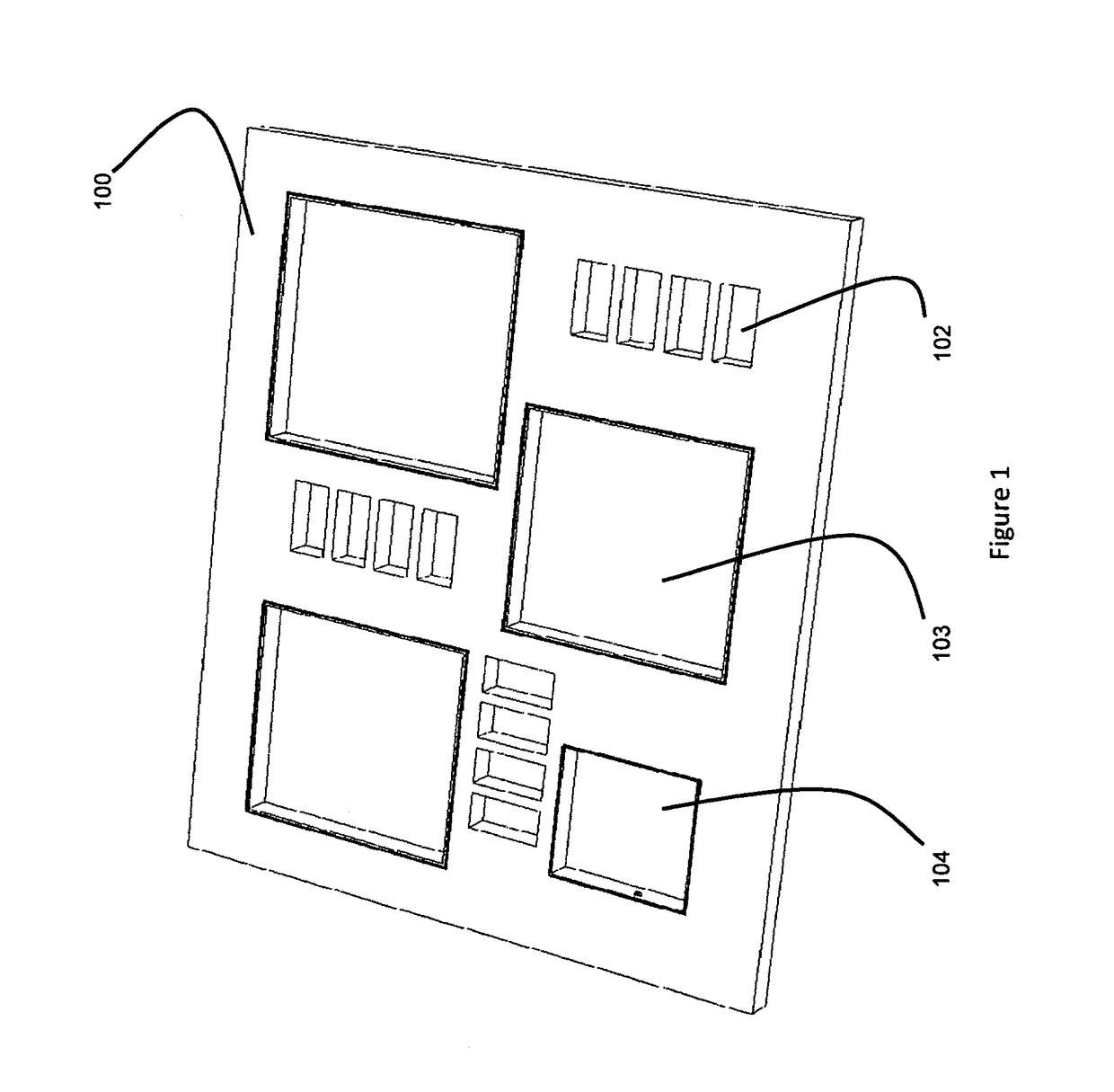
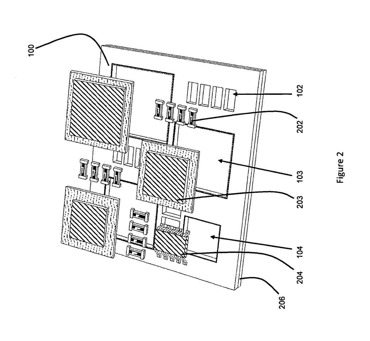
[0030]FIG. 1 shows a frame 100 with apertures 102, 103, and 104 into which electrical components may be inserted. The frame 100 may be continuous, sectioned, in multiple discrete pieces or temporarily attached to other pieces of frame in anticipation of creating a finished structure which will have flexible areas in the completed assembly to allow for subsequent folding or bending of the assembly. FIG. 2 shows electrical components (for example discrete component 202, land grid array component 203, and gull wing component 204) in position over respective apertures 102, 103, and 104 of frame 100. Frame 100 sits on a substrate 206 which may be either temporarily or permanently attached to frame 100.

[0031]FIG. 3 shows a section of frame 100 situated on substrate 206 with components 202, 203, and 204 inserted into respective apertures 102, 103, and 104 and attached to substrate 206.

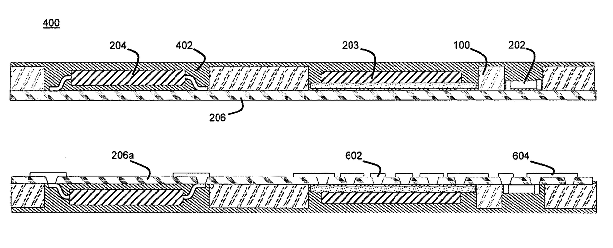
[0032]FIG. 4 shows subassembly 400, including frame 100 and substrate 206, with electrically insulating ma...


PUM

PropertyMeasurementUnit
temperaturesaaaaaaaaaa
insulatingaaaaaaaaaa
electrically insulatingaaaaaaaaaa

Abstract

A frame 100 containing aperture(s) 102, 103, 104 is positioned on and joined to a permanent substrate 206a or temporary substrate 206b. Electrical component(s) 202, 203, 204 are placed into respective aperture(s) 102, 103, 104 with the leads 504, 1002 of the component(s) 202, 203, 204 positioned on and attached to the permanent substrate 206a or the temporary substrate 206b. Then an encapsulant 402, electrically insulating, but preferably thermally conductive, envelops the component(s) 102, 103, 104. At this point, temporary substrate 206b may be removed exposing component leads 1002. Or, if component(s) 102, 103, 104 are mounted on permanent substrate 206a, vias 502 extend from the surface of substrate 206a to leads 504. With leads 504, 1002 exposed, the completed subassembly 500, 1000 may be incorporated into various forms of reverse-interconnection process (RIP) assemblies as detailed in related applications.

Description

CROSS-REFERENCE TO RELATED APPLICATIONS[0001]This application claims the benefit of U.S. Provisional Application No. 60 / 966,643, filed on Aug. 28, 2007, hereby incorporated by reference in its entirety; U.S. Provisional Application No. 61 / 038,564, filed on Mar. 21, 2008, hereby incorporated by reference in its entirety; U.S. Provisional Application No. 61 / 039,059 filed on Mar. 24, 2008, hereby incorporated by reference in its entirety; and U.S. Provisional Application No. 61 / 075,238 filed on Jun. 24, 2008, hereby incorporated by reference in its entirety.[0002]This application is a continuation-in-part application of pending U.S. patent application Ser. No. 12 / 119,287, ELECTRONIC ASSEMBLIES WITHOUT SOLDER AND METHODS FOR THEIR MANUFACTURE; U.S. patent application Ser. No. 12 / 163,870, ELECTRONIC ASSEMBLIES WITHOUT SOLDER AND METHODS FOR THEIR MANUFACTURE; U.S. patent application Ser. No. 12 / 191,544, ELECTRONIC ASSEMBLIES WITHOUT SOLDER AND METHODS FOR THEIR MANUFACTURE; U.S. patent a...

Claims


Application Information

Patent Timeline
Patent Type & Authority Patents(United States)
IPC IPC(8): H05K1/18H05K1/05H05K3/28H05K3/46
CPCH05K1/185H01L2924/14H01L2924/3025H05K1/056H05K3/284H05K3/4644H05K2201/0969H05K2201/2018H05K2203/0156H05K2203/1469Y10T29/49124Y10T29/49146H01L2924/00H01L21/568H01L2224/04105H01L2224/92144H01L2224/96H01L2924/19105
Inventor FJELSTAD, JOSEPH C.
Owner FJELSTAD JOSEPH CHARLES
Why Eureka
Try Eureka