Micromechanical pressure sensor device and corresponding manufacturing method

a pressure sensor and micro-mechanical technology, applied in the direction of generator/motor, television system, instruments, etc., can solve the problems of increasing complexity and cost of packaging the pressure sensor, and achieve the effect of increasing the signal sensitivity of the capacitive pressure sensor devi

Active Publication Date: 2017-07-18
ROBERT BOSCH GMBH
View PDF60 Cites 7 Cited by
  • Summary
  • Abstract
  • Description
  • Claims
  • Application Information

AI Technical Summary

Benefits of technology

[0012]The micromechanical pressure sensor device and the corresponding manufacturing method according to the present invention cause an increased signal sensitivity of a capacitive pressure sensor device. The manufacturing method at the same time allows capacitive acceleration, rotation rate and / or magnetic field sensors to be produced on the same chip and thus a 7D or 10D integration to be achieved.
[0015]As an alternative to increasing the signal sensitivity compared to known systems, the present invention allows the space requirement for the diaphragm area to be considerably reduced, i.e., greater integration to be achieved.
[0016]According to one preferred refinement, the plug-like joining area is formed centrally on the diaphragm area, so that the first pressure detection electrode may be deflected essentially untilted. In this way a maximal signal deviation is achievable.
[0020]According to one further preferred refinement, the deflectable first pressure detection electrode is formed in the second micromechanical functional layer, the fixed second pressure detection electrode being formed in a capping device, which is bonded to the MEMS wafer. Such a structure is very easy to produce.
[0024]According to one further preferred refinement, a capping device is provided, which is bonded to the second micromechanical functional layer for enclosing a cavern at a predetermined enclosed pressure. In this way, an arbitrary reference pressure may be set.
[0025]According to one further preferred refinement, the capping device is an evaluation wafer. This results in a very compact system.

Problems solved by technology

One essential reason for this is the necessary media access which a pressure sensor requires, contrary to inertial and magnetic sensors, and which considerably increases the complexity and the costs for packaging the pressure sensor.

Method used


Image

  • Micromechanical pressure sensor device and corresponding manufacturing method
  • Micromechanical pressure sensor device and corresponding manufacturing method
  • Micromechanical pressure sensor device and corresponding manufacturing method

Examples


Embodiment Construction

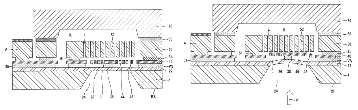
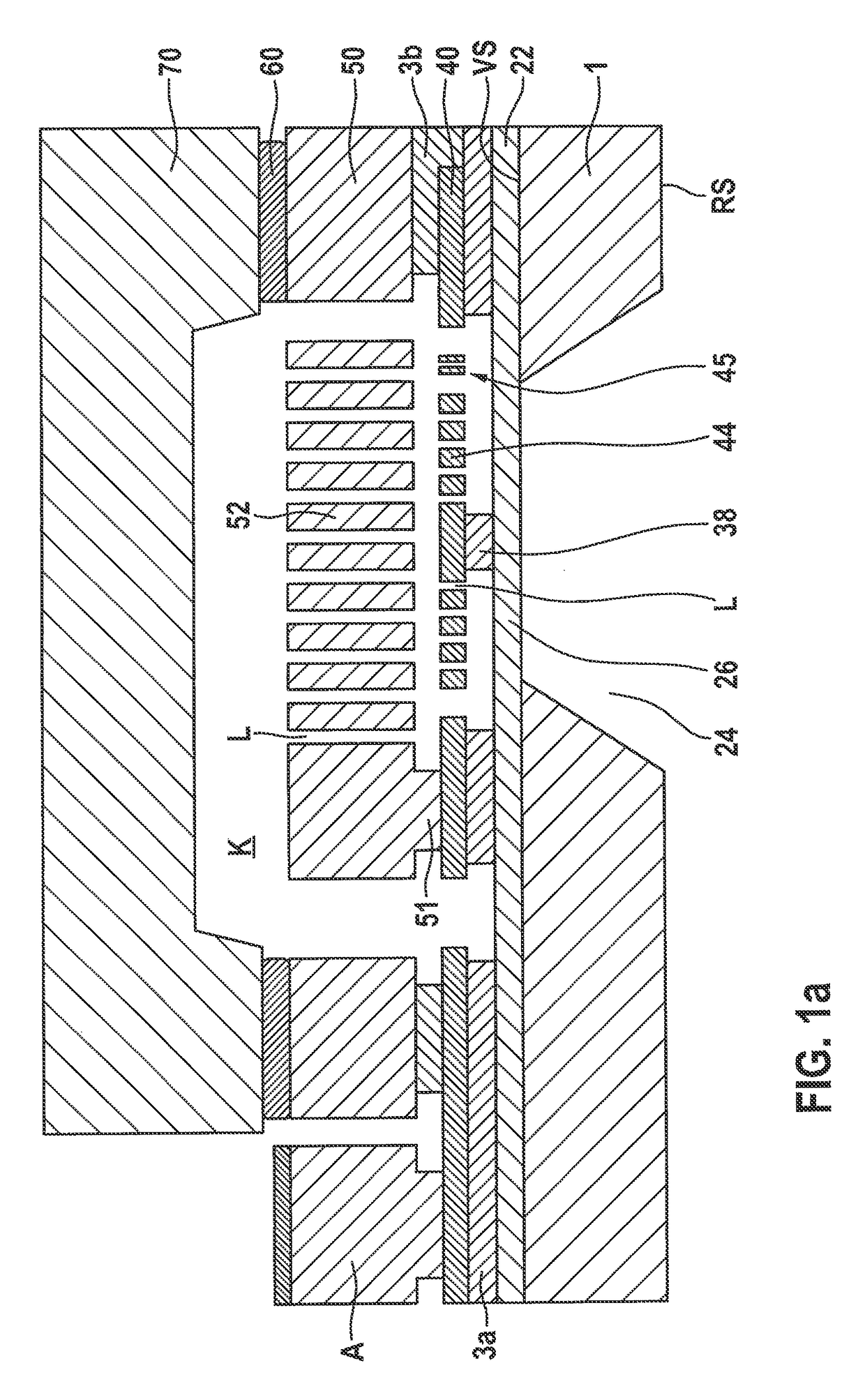
[0039]In the figures, identical or functionally equivalent elements are denoted by identical reference numerals.

[0040]FIGS. 1a) and 1b) show schematic cross-sectional views to explain a micromechanical pressure sensor device and a corresponding manufacturing method according to a first specific embodiment of the present invention.

[0041]In FIGS. 1a) and 1b) reference numeral 1 denotes an MEMS wafer made of silicon, which has a front side VS and a rear side RS. A highly doped cover layer 22 is applied to front side VS of MEMS wafer 1, at which a KOH etching step starting from rear side RS for forming an access opening 24, which hereafter is also referred to as a through-hole, comes to a stop. In this way, it is possible to expose, from rear side RS, a diaphragm area 26 having the thickness of cover layer 22.

[0042]From front side VS, a first micromechanical functional layer 40 and a second micromechanical functional layer 50, which are each made of silicon, are structured and exposed u...


PUM

PropertyMeasurementUnit
pressureaaaaaaaaaa
rotation rateaaaaaaaaaa
magnetic fieldaaaaaaaaaa

Abstract

A micromechanical pressure sensor device includes: an MEMS wafer having a front side and a rear side; a first micromechanical functional layer formed above the front side of the MEMS wafer; and a second micromechanical functional layer formed above the first micromechanical functional layer. A deflectable first pressure detection electrode is formed in one of the first and second micromechanical functional layers. A fixed second pressure detection electrode is formed spaced apart from and opposite the deflectable first pressure detection electrode. An elastically deflectable diaphragm area is formed above the front side of the MEMS wafer. An external pressure is applied to the diaphragm area via an access opening in the MEMS wafer, and the wafer is connected to the deflectable first pressure detection electrode via a plug-like joining area.

Description

BACKGROUND OF THE INVENTION[0001]1. Field of the Invention[0002]The present invention relates to a micromechanical pressure sensor device and to a corresponding manufacturing method.[0003]2. Description of the Related Art[0004]While any arbitrary micromechanical components may also be used, the present invention and the problems underlying the present invention are explained based on silicon-based components.[0005]Micromechanical sensor devices for measuring acceleration, rotation rate, magnetic field and pressure, for example, are generally known and are manufactured for various applications in the automotive and consumer fields in mass production. Trends in the consumer electronics are in particular the miniaturization of the components, the integration of functions, and effective cost reduction.[0006]Today, acceleration and rotation rate sensors and also acceleration and magnetic field sensors are already manufactured as combination sensors (6d), and additionally the first 9d mod...

Claims


Application Information

Patent Timeline
Patent Type & Authority Patents(United States)
IPC IPC(8): G01L9/00B81B7/02B81B3/00B81C1/00G01P15/08G01P15/125
CPCG01L9/0072B81B3/0037B81B7/02B81C1/00158B81C1/00246G01P15/0802G01P15/125B81B2201/025B81B2201/0264
Inventor KAELBERER, ARNDREINMUTH, JOCHENCLASSEN, JOHANNES
Owner ROBERT BOSCH GMBH
Why Eureka
Try Eureka