Optoelectronic modules having a silicon substrate, and fabrication methods for such modules

a technology of optoelectronic modules and silicon substrates, which is applied in the direction of electrical equipment, semiconductor devices, radio frequency control devices, etc., can solve the problems of poor heat transfer of modules, degrading of module optical properties, etc., and achieves relatively high thermal conductivity of silicon, small footprint, and reduced overall cost of modules

Active Publication Date: 2017-07-18
AMS SENSORS SINGAPORE PTE LTD
View PDF12 Cites 6 Cited by
  • Summary
  • Abstract
  • Description
  • Claims
  • Application Information

AI Technical Summary

Benefits of technology

[0006]One or more of the following advantages are provided by some implementations. For example, by using a silicon substrate in which various electronic and/or optoelectronic components can be formed, the module can have as a relatively small footprint. The overall cost of the module can be reduced in some cases by eliminating the need for (and cost of) a printed circuit board substrate. Likewise, in some instances, a...

Problems solved by technology

Further, poor transfer of heat away from the modules can be problematic in some cases.
Likewise, in some...

Method used


Image

  • Optoelectronic modules having a silicon substrate, and fabrication methods for such modules
  • Optoelectronic modules having a silicon substrate, and fabrication methods for such modules
  • Optoelectronic modules having a silicon substrate, and fabrication methods for such modules

Examples


Embodiment Construction

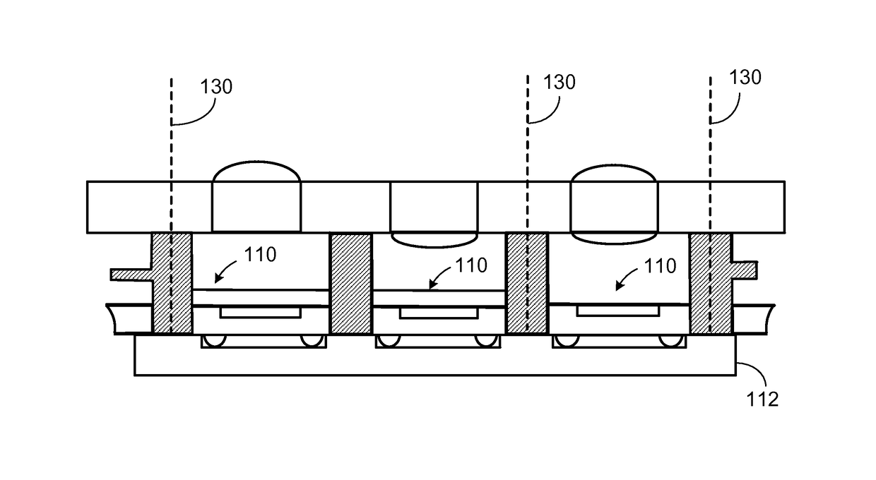
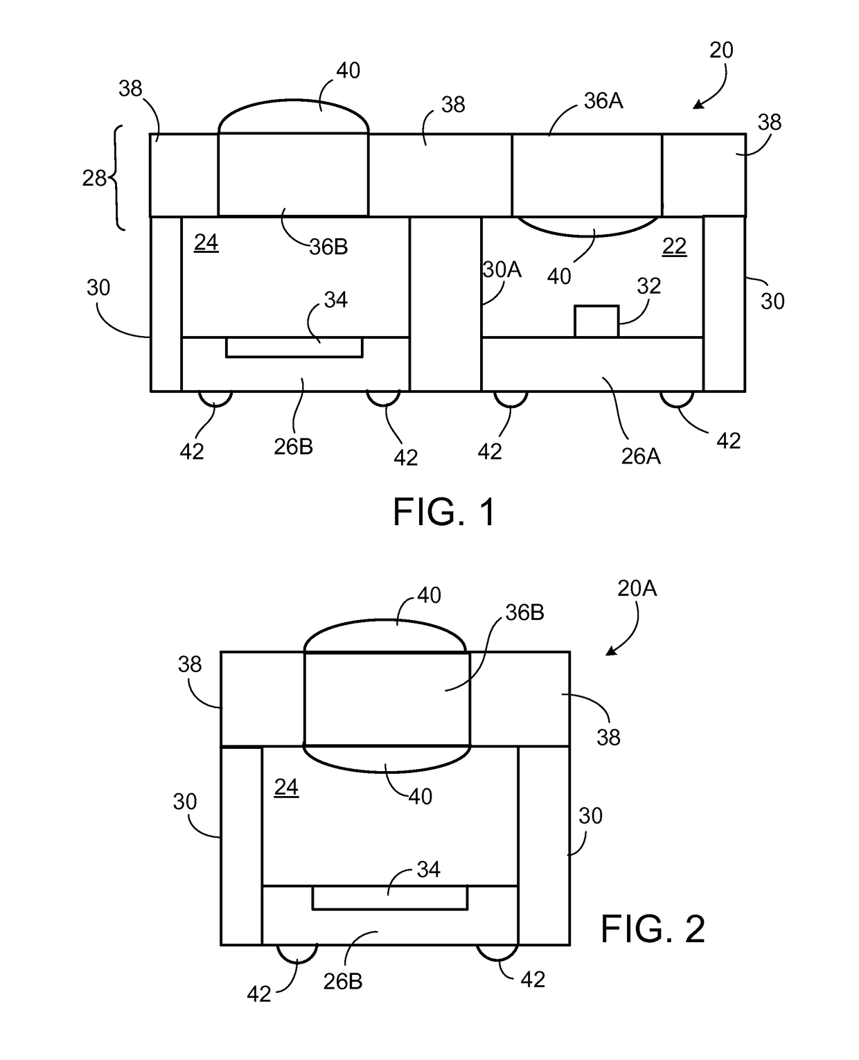
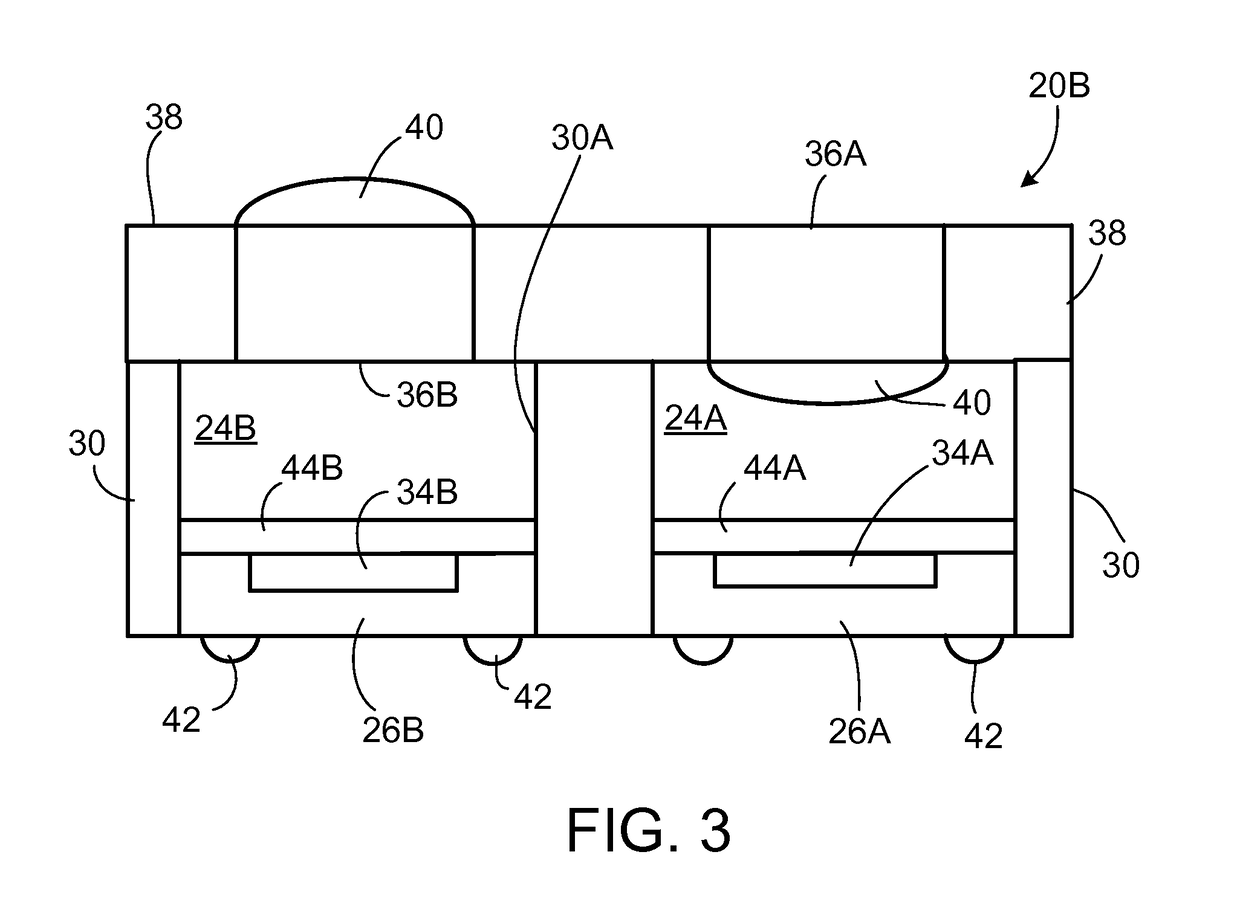
[0022]As shown in FIG. 1, a first example of an optoelectronic module 20 includes an array of optical channels. In the illustrated example, the module 20 includes an emission channel 22 and a detection channel 24. The module 20 has silicon substrates 26A, 26B, which are separated from an optics assembly 28 by a spacer 30. Thus, interior regions of the module 20 are bounded by the substrates 26A, 26B, the spacer 30 and the optics assembly 28.

[0023]Different portions of each silicon substrate 26A, 26B may exhibit different electronic and / or optoelectronic properties. A respective active optoelectronic device is integrated in, or disposed on, each silicon substrate 26A, 26B. For example, a light emitting element 32 (e.g., a LED, a laser diode or a series of LEDs or laser diodes) can be formed in, or mounted on, the silicon substrate 26A in the emission channel 22. Likewise, a single light detecting element (e.g., a photodiode) or an array of light detecting elements 34 (e.g., pixels of...


PUM


Abstract

Optoelectronic modules include a silicon substrate in which or on which there is an optoelectronic device. An optics assembly is disposed over the optoelectronic device, and a spacer separates the silicon substrate from the optics assembly. Methods of fabricating such modules also are described.

Description

CROSS-REFERENCE TO RELATED APPLICATIONS[0001]This application claims the benefit of U.S. Provisional Application No. 62 / 039,028, filed Aug. 19, 2014 and U.S. Provisional Application No. 62 / 056,897, filed Sep. 29, 2014, all of which are incorporated herein by reference in their entirety.FIELD OF THE DISCLOSURE[0002]This disclosure relates to optoelectronic modules having a silicon substrate, and fabrication methods for such modules.BACKGROUND[0003]Smartphones and other devices sometimes include miniaturized optoelectronic modules such as light modules, sensors or cameras. Light modules can include a light emitting element such as a light emitting diode (LED), an infra-red (IR) LED, an organic LED (OLED), an infra-red (IR) laser or a vertical cavity surface emitting laser (VCSEL) that emits light through a lens to outside the device. Other modules can include a light detecting element. For example, CMOS and CCD image sensors can be used in primary or front facing cameras. Likewise, pr...

Claims


Application Information

Patent Timeline
IPC IPC(8): H01L33/00H01L27/146
CPCH01L27/14625H01L27/14618H01L27/14621H01L27/14685
Inventor RUDMANN, HARTMUTCESANA, MARIOGEIGER, JENSROENTGEN, PETERCONDORELLI, VINCENZO
Owner AMS SENSORS SINGAPORE PTE LTD
Why Eureka
Try Eureka