
Reactive monomer, a liquid crystal panel and an electronic equipment

a liquid crystal panel and reactive monomer technology, applied in the field of optical material technology, can solve the problems of productivity decline, achieve the effects of accelerating the polymerization of reactive monomers, improving reaction rate, and shortening illumination tim

Active Publication Date: 2017-08-08
TCL CHINA STAR OPTOELECTRONICS TECH CO LTD
View PDF7 Cites 0 Cited by
  • Summary
  • Abstract
  • Description
  • Claims
  • Application Information

AI Technical Summary

Benefits of technology

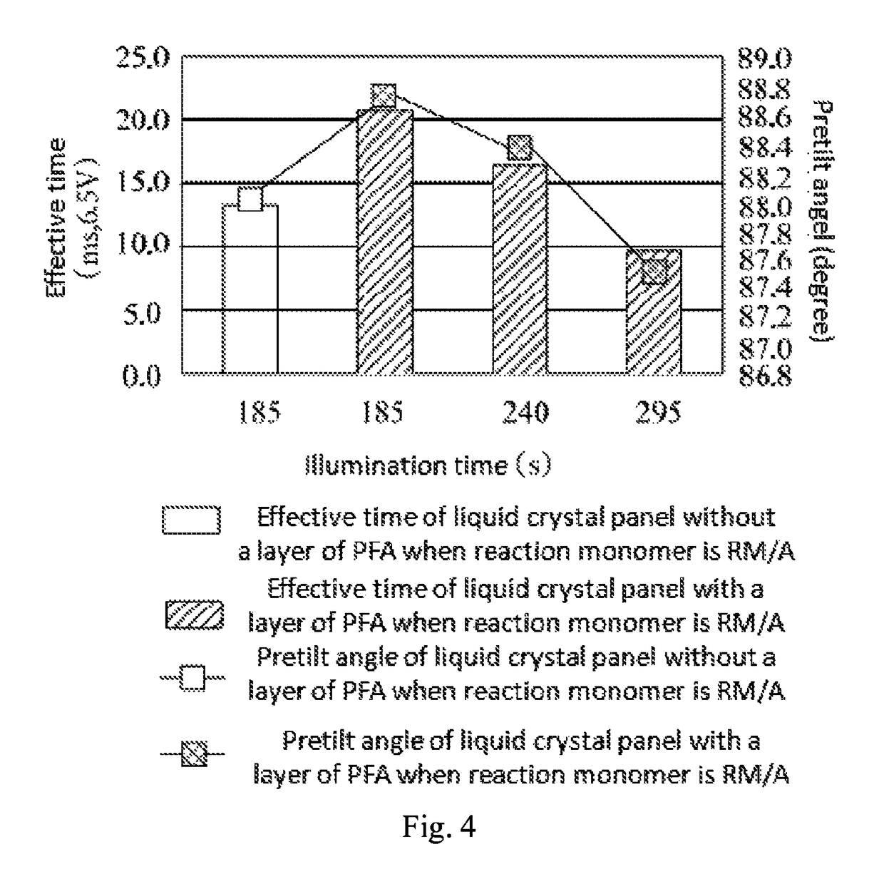
[0018]The advantageous effects of the invention are: the situation is different from the prior art, that by utilizing the reactive monomer with plentiful biphenyl structures which is even more sensitive to ultra violet light so that absorbing ultra violet light more effectively, and energy inside molecule can be passed to the polymerizable groups at both sides after absorbing the ultra violet light to accelerate polymerization of the reactive monomer and to get a better reaction rate, so that shortening illumination time during manufacturing and increasing production efficiency.
of the invention are: the situation is different from the prior art, that by utilizing the reactive monomer with plentiful biphenyl structures which is even more sensitive to ultra violet light so that absorbing ultra violet light more effectively, and energy inside molecule can be passed to the polymerizable groups at both sides after absorbing the ultra violet light to accelerate polymerization of the reactive monomer and to get a better reaction rate, so that shortening illumination time during manufacturing and increasing production efficiency.

Problems solved by technology

However, an effect of productivity decreases because the illumination time of the UV1 is too long.

Method used


Image

  • Reactive monomer, a liquid crystal panel and an electronic equipment
  • Reactive monomer, a liquid crystal panel and an electronic equipment
  • Reactive monomer, a liquid crystal panel and an electronic equipment

Examples


Embodiment Construction

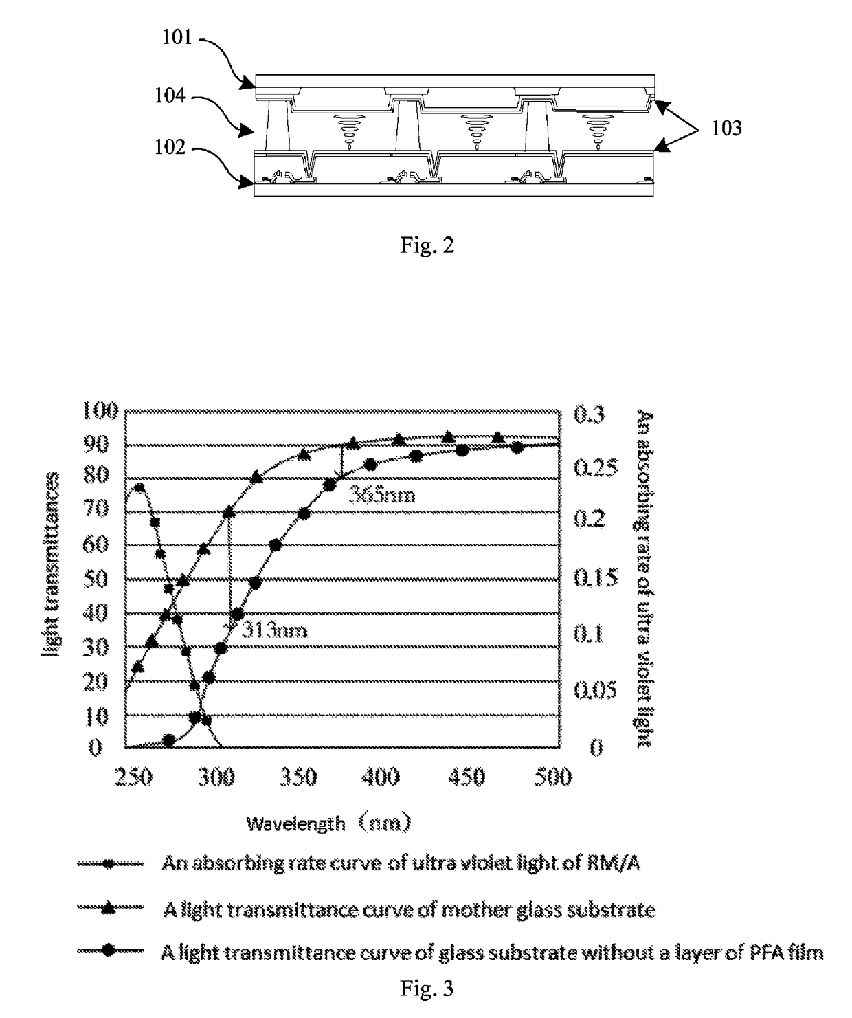
[0035]Please refer to FIG. 2, FIG. 2 is a structural schematic view of an implementation plan of a liquid crystal panel in the invention.

[0036]The liquid crystal panel comprises a first substrate 101, a second substrate 102 and a liquid crystal layer 104 disposed between the first substrate 101 and the second substrate 102, and the liquid crystal layer 104 comprises a liquid crystal compound which comprises a reactive monomer (hereinafter referred to as RM / B).

[0037]Both corresponding sides of the first substrate 101 and the second substrate 102 dispose alignment films 3 respectively. In this embodiment, the first substrate 101 is a color filter substrate (CF), the second substrate is a thin film transistor array substrate (TFT), and the alignment film 103 is a vertical alignment film. RM / B of the liquid crystal compound of the liquid crystal layer 104 comprises a biphenyl structure and polymeriable groups connecting at both sides of the biphenyl structure, a formula I of the reactiv...


PUM

PropertyMeasurementUnit
timeaaaaaaaaaa
illumination timeaaaaaaaaaa
wavelengthaaaaaaaaaa

Abstract

The invention discloses a reactive monomer, a liquid crystal panel and an electronic equipment. The reactive monomer comprises a biphenyl structure and polymeriable groups connecting at both sides of the biphenyl structure, a structure of the reactive monomer iswherein, n≧3 B are the polymerizable groups;the liquid crystal panel in the invention comprises both a first substrate and a second substrate with disposed alignment films respectively, and a liquid crystal layer disposed between the first substrate and the second substrate, and the liquid crystal layer comprises the liquid crystal compound which comprises the reactive monomer. The reactive monomer in the invention can absorb ultra violet light more efficiently, shorten an illuminating time of UV1, and increase production efficiency.

Description

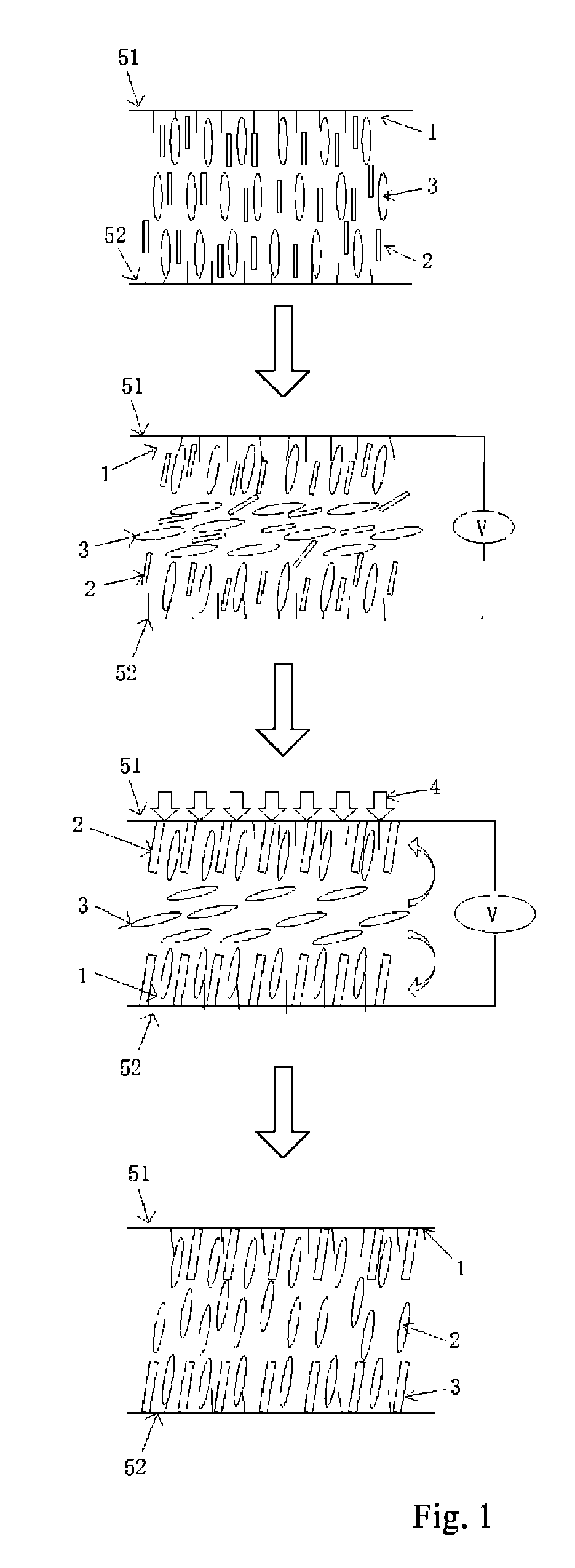
FIELD OF THE INVENTION[0001]The invention relates to an optical material technology field, particularly to a reactive monomer, and both a liquid crystal panel and an electronic equipment with the reactive monomer.BACKGROUND OF THE INVENTION[0002]PSVA (Polymer stabilized vertical alignment) technology is a stable vertical alignment technology of polymer, and the biggest feature herein is utilizing VA liquid crystal to form a pretilt angle of polymer layer on a alignment film 1 (PI).[0003]The concrete forming process comprises four steps as shown in FIG. 1, (1): adding a certain ratio of polymerizable reactive monomer 2 (RM, Reactive monomer) in a liquid crystal medium, and the reactive monomer 2 is polymerized into macromolecule network after illuminated by ultra violet light; (2) before illuminating by UV light 4, adding a voltage between up-substrate 51 and down-substrate 52 to form a liquid crystal molecule 3 a pretilt angel; (3) illuminating by particular UV light 4 after stabili...

Claims


Application Information

Patent Timeline
Patent Type & Authority Patents(United States)
IPC IPC(8): G02F1/1333C09K19/12C09K19/38G02F1/1368G02F1/1335C07C69/54G02F1/1337C07C69/653C09K19/04
CPCC09K19/12C07C69/54C07C69/653C09K19/3804G02F1/1337G02F1/1368G02F1/133365G02F1/133514C09K2019/0448C09K2019/123G02F2001/133302G02F2001/133742G02F2202/022G02F1/1333G02F1/133711G02F1/133742G02F1/133302
Inventor LI, XIANGSONG, YANJUNHSIEH, CHUNG-CHING
Owner TCL CHINA STAR OPTOELECTRONICS TECH CO LTD
Learn More