Light-erasable embedded memory device and method of manufacturing the same

a technology of embedded memory and light-erasing, which is applied in the field of memory devices, can solve the problems of difficulty in storing electrons in the semiconductor process, and achieve the effect of less process steps or costs and high process integration

Active Publication Date: 2017-08-08
UNITED MICROELECTRONICS CORP
View PDF2 Cites 8 Cited by
  • Summary
  • Abstract
  • Description
  • Claims
  • Application Information

AI Technical Summary

Benefits of technology

[0012]It is a novel process concept to forma light permeable passage in the semiconductor device by using existing semiconductor processes with high process integration and less process step or cost.

Problems solved by technology

While the semiconductor device, such as CMOS, BJT, or diode, is mostly operated by electrical signals, how to integrate the OTPROM process which uses UV light to erase the stored electrons in the semiconductor process is still a challenge in the industry.

Method used


Image

  • Light-erasable embedded memory device and method of manufacturing the same
  • Light-erasable embedded memory device and method of manufacturing the same
  • Light-erasable embedded memory device and method of manufacturing the same

Examples


Embodiment Construction

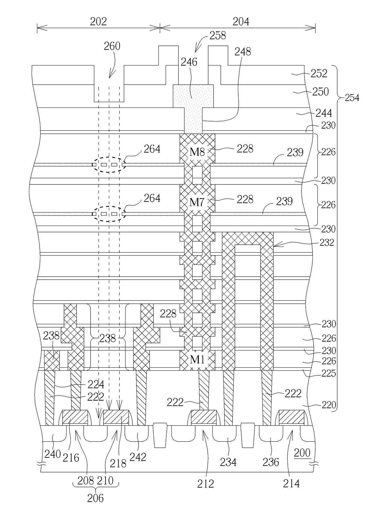
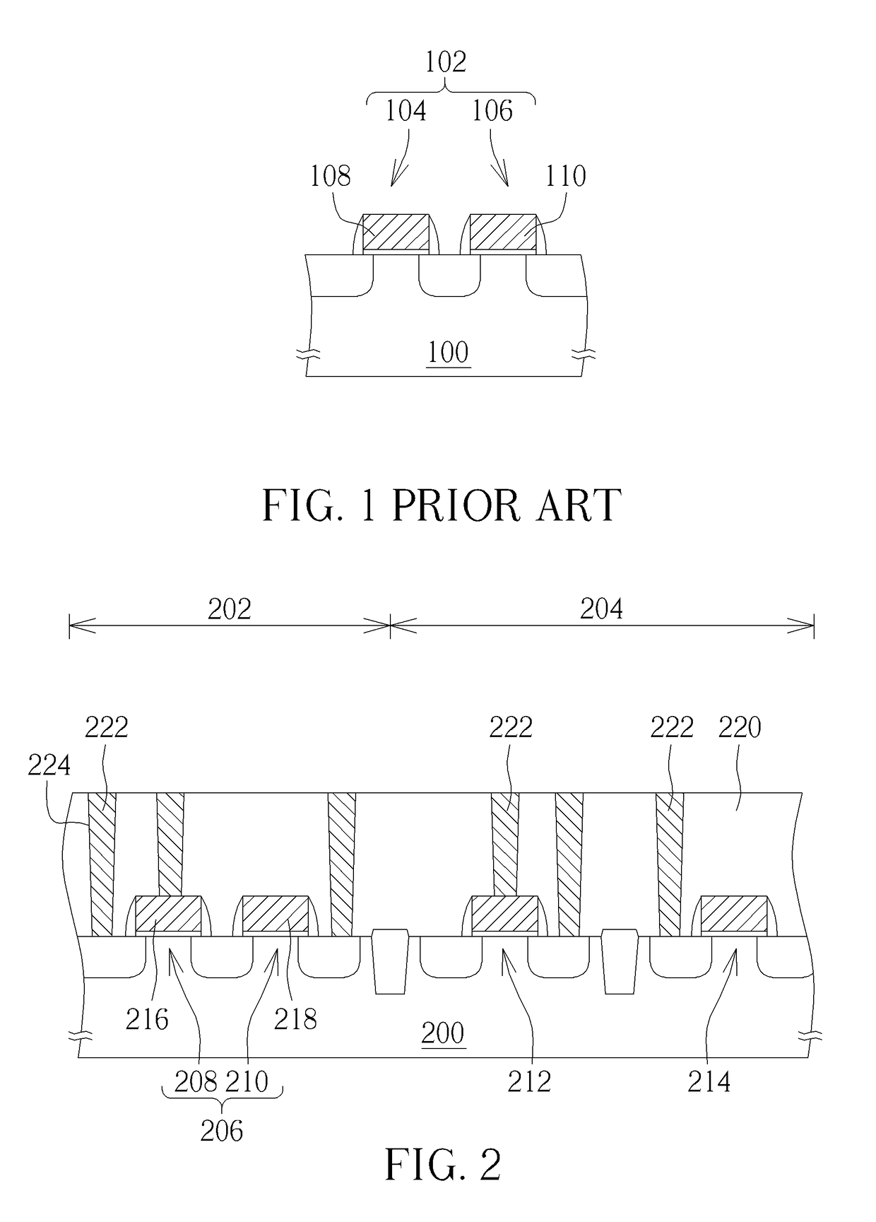
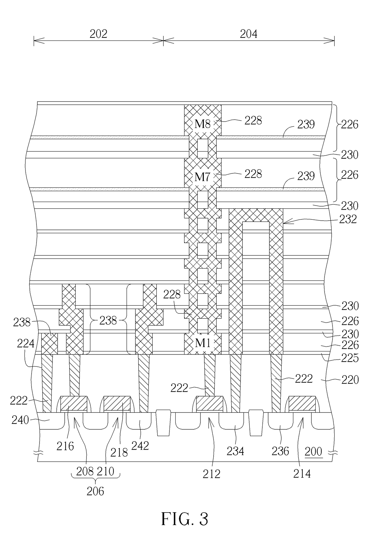
[0025]Advantages and features of embodiments may be understood more readily by reference to the following detailed description of preferred embodiments and the accompanying drawings. Embodiments may, however, be embodied in many different forms and should not be construed as being limited to those set forth herein. Rather, these embodiments are provided so that this disclosure will be thorough and complete and will fully convey exemplary implementations of embodiments to those skilled in the art, so embodiments will only be defined by the appended claims. Like reference numerals refer to like elements throughout the specification.

[0026]The terminology used herein is for the purpose of describing particular embodiments only and is not intended to be limiting. As used herein, the singular forms “a”, “an” and “the” are intended to include the plural forms as well, unless the context clearly indicates otherwise. It will be further understood that the terms “comprises” and / or “comprising...


PUM


Abstract

A light-erasable embedded memory device and a method for manufacturing the same are provided in the present invention. The light-erasable embedded memory device includes a substrate with a memory region and a core circuit region, a floating gate on the memory region of the substrate, at least one light-absorbing film above the floating gate, wherein at least one light-absorbing film is provided with dummy via holes overlapping the floating gate, and a dielectric layer on the light-absorbing film and filling up the dummy via holes.

Description

BACKGROUND OF THE INVENTION[0001]1. Field of the Invention[0002]The present invention relates to a memory device and a fabricating method thereof. More particularly, the present invention relates to an illuminating efficiency-increasable and light-erasable embedded memory device and a fabricating method thereof.[0003]2. Description of the Prior Art[0004]A memory is a semiconductor device used for storing data or information. The requirements for memory are getting higher and higher along with the advancement in the function of computer micro-processors and the increase in volume of software programs and calculations. The technique and the process for fabricating memory devices with large-volume and low-cost memory have been driving the semiconductor technology to go towards high integration constantly.[0005]Among various memory products, a non-volatile memory has been applied widely to personal computers and other electronic equipment in which data can be read from, written to, or e...

Claims


Application Information

Patent Timeline
Patent Type & Authority Patents(United States)
IPC IPC(8): H01L21/336H01L27/11521G11C16/04H01L29/51H01L23/528H01L21/268H01L21/28H01L23/522
CPCG11C16/0416H01L27/11521H01L29/518H01L21/28273H01L21/2686H01L23/528H01L23/5226G11C16/0433G11C16/18G11C17/143G11C2216/26H10B41/49H10B41/30
Inventor SU, HAOLIM, CHOW YEEJIANG, CHAOLIAO, HONG
Owner UNITED MICROELECTRONICS CORP
Why Eureka
Try Eureka