Method of cyclic dry etching using etchant film

a technology of etching film and etchant, which is applied in the direction of basic electric elements, semiconductor/solid-state device manufacturing, electric devices, etc., can solve the problems of poor in-plane uniformity of etching of a film on a substrate by etchant, inability to achieve good in-plane uniformity of etching, and suffer from in-plane uniformity. achieve the effect of high controllability

Active Publication Date: 2017-10-17
ASM IP HLDG BV
View PDF1599 Cites 311 Cited by
  • Summary
  • Abstract
  • Description
  • Claims
  • Application Information

AI Technical Summary

Benefits of technology

[0011]In some embodiments, the target layer can be constituted by any material (e.g., TiO2) which can be etched using fluorine, i.e., by using a CF film. In some embodiments, the target layer can be constituted by a material which can be etched using a halogen other than fluorine, as long as a suitable etchant film is selected. Typically, the etchant film is exposed to an oxygen plasma in a reactive ion etching (ME) process. Since the etching process involves a self-limiting reaction process (or saturation process), high controllability can be realized.

Problems solved by technology

However, it is revealed that in-plane uniformity of etching of a film on a substrate by ALE is not satisfactory when etching an oxide or nitride mineral film such as silicon oxide or nitride film.
However, when etching a silicon oxide or silicon nitride film by ALE using a fluorocarbon such as C4F8 as an etchant gas, good in-plane uniformity of etching is not obtained.
As a result, in-plane uniformity of etching suffers.
However, none of conventional etchant gases satisfies the above.
Similarly, the depth of the etched portion of the target layer increases as the duration of exposure of the etchant film to the plasma increases; however, the depth of the etched portion reaches a plateau and no longer increases when the duration of exposure of the etchant film to the plasma reaches a certain value.

Method used


Image

  • Method of cyclic dry etching using etchant film
  • Method of cyclic dry etching using etchant film
  • Method of cyclic dry etching using etchant film

Examples


example 1

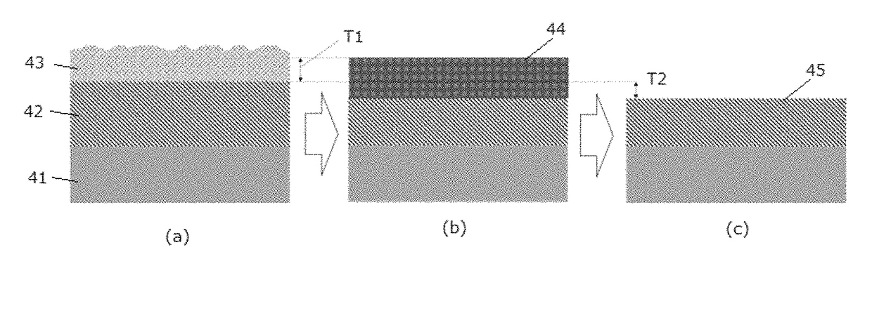
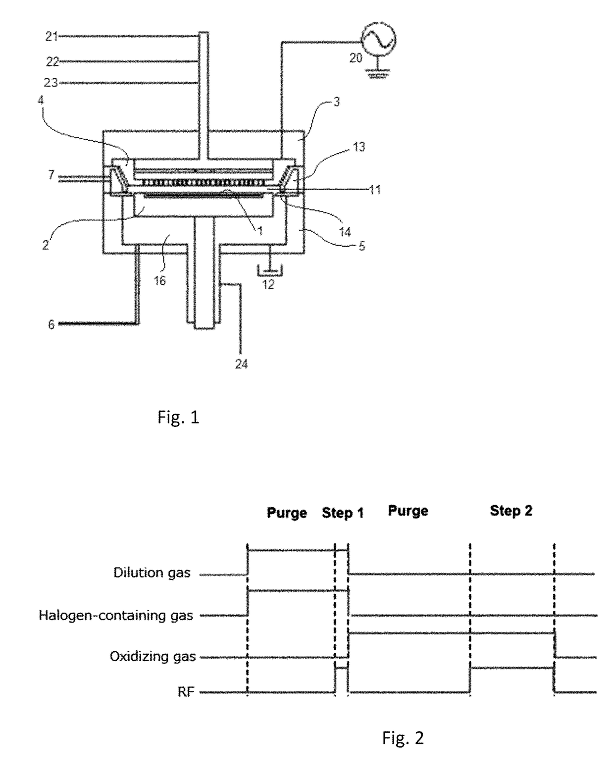
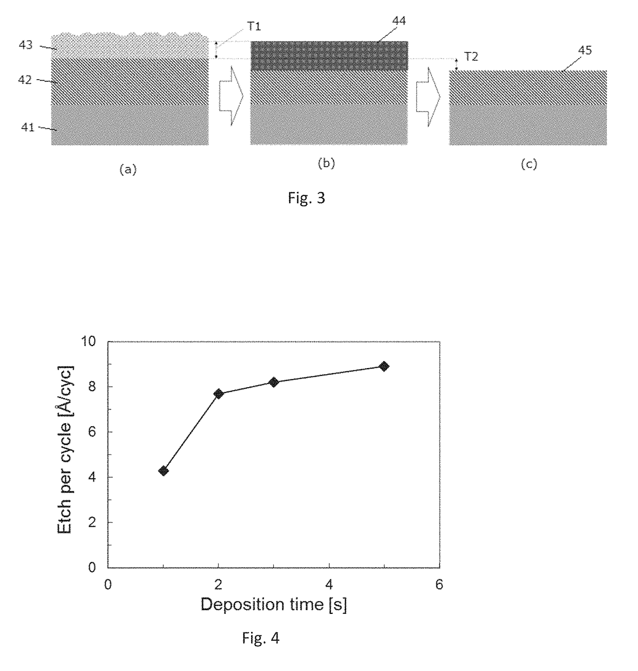
[0051]A silicon oxide film was formed at a thickness of 24 nm by PEALD on a 300-mm substrate. In Example 1, deposition of an etchant film and etching of the silicon oxide film were conducted under the conditions shown in Table 2 below using the plasma-assisted etching apparatus illustrated in FIG. 1. The sequence used in each etching cycle is shown in FIG. 2.

[0052]

TABLE 2(numbers are approximate)Conditions for depositionSubstrate temperature20° C.Pressure2.0 PaDeposition gasC4F8Noble gas (as a carrier gas Arand / or dilution gas)Flow rate of deposition gas10 sccm(etchant gas) (continuous)Flow rate of dilution gas90 sccm(continuous)RF power for a 300-mm wafer100 W; 60 MHzDuration of “Purge”120 secDuration of “RF” (Step 1)See FIG. 4 (“Deposition time [s]”)Growth rate per cycle (Å / cycle)6.9Film thickness (Å)6.9Conditions for etchingSubstrate temperature20° C.Pressure2.0 PaEtching gasO2Flow rate of etching gas50 sccm(continuous)RF power for a 300-mm wafer100 W; 60 MHzDuration of “Purge”12...

example 2

[0055]The etching process was performed in Example 2 according to Example 1 above, except that the deposition time (the duration of “RF” (Step 1)) was set at 2 seconds, and the etching time (the duration of “RF” (Step 2)) varied as shown in FIG. 5. FIG. 5 is a graph showing the relationship between etching rate per cycle (EPC) ({acute over (Å)} / cycle) and etching time per cycle (seconds) in Example 2.

[0056]FIG. 5 indicates that the depth of the etched portion of the silicon oxide layer (“Etch per cycle [{acute over (Å)} / cyc]”) increased as the etching time (“Etching time [s]”) increased; however, the depth of the etched portion reached a point near a plateau which is defined as a point where the depth of an etched portion no longer increases even when the etching time increases. This is because etching reaction took place only when the etchant film existed, and etching stopped when the etchant film was removed. In the above, in principle, “a point near a plateau” can be defined as a...

example 3

[0057]The etching process was performed in Example 3 according to Example 1 above, except that the deposition time (the duration of “RF” (Step 1)) was set at 2 seconds, the etching time (the duration of “RF” (Step 2)) was set at 60 seconds, and the number of etching cycles repeated varied as shown in FIG. 6. FIG. 6 is a graph showing the relationship between thickness of the SiO2 layer (nm) and number of cycles repeated in an etching process in Example 3.

[0058]FIG. 6 indicates that the thickness of the etchant film “depth of the etched portion of the silicon oxide layer (“SiO2 thickness (nm)”) decreased proportionally to the increase of the number of etching cycles (“Cycle number”). The relationship between the above two is substantially linear. That is, controllability of the etching process was very high since the etching process used a self-limiting or saturation process.


PUM


Abstract

A method for etching a target layer on a substrate by a dry etching process includes at least one etching cycle, wherein an etching cycle includes: depositing a halogen-containing film using reactive species on the target layer on the substrate; and etching the halogen-containing film using a plasma of a non-halogen etching gas, which plasma alone does not substantially etch the target layer, to generate etchant species at a boundary region of the halogen-containing film and the target layer, thereby etching a portion of the target layer in the boundary region.

Description

BACKGROUND[0001]Field of the Invention[0002]The present invention generally relates to a method of cyclic dry etching of a layer constituted by silicon or metal oxide, nitride, or carbide.[0003]Description of the Related Art[0004]Atomic layer etching (ALE) is cyclic, atomic layer-level etching using an etchant gas adsorbed on a target film and reacted with excited reaction species, as disclosed in Japanese Patent Laid-open Publication No. 2013-235912 and No. 2014-522104. As compared with conventional etching technology, ALE can perform precise, atomic layer-level continuous etching on a sub-nanometer order to form fine, narrow convex-concave patterns and may be suitable for e.g., double-patterning processes. As an etchant gas, Cl2, HCl, CHF3, CH2F2, CH3F, H2, BCL3, SiCl4, Br2, HBr, NF3, CF4, C2F6, C4F8, SF6, O2, SO2, COS, etc. are known. However, it is revealed that in-plane uniformity of etching of a film on a substrate by ALE is not satisfactory when etching an oxide or nitride mi...

Claims


Application Information

Patent Timeline
Patent Type & Authority Patents(United States)
IPC IPC(8): H01L21/311H01L21/02
CPCH01L21/31116H01L21/02274H01L21/02118H01L21/0212H01L21/30655H01L21/3065H01L21/32136H01L21/0228
Inventor ZAITSU, MASARUKOBAYASHI, NOBUYOSHIKOBAYASHI, AKIKOHORI, MASARUKONDO, HIROKITSUTSUMI, TAKAYOSHI
Owner ASM IP HLDG BV
Why Eureka
Try Eureka