Broad area laser including anti-guiding regions for higher-order lateral mode suppression

a laser diode and wide area technology, applied in lasers, laser details, electrical equipment, etc., can solve the problems of ever increasing lateral divergence, limited use of output beams in materials processing applications, and the ability of output beams to focus, so as to achieve high beam quality

Active Publication Date: 2017-10-24
II VI DELAWARE INC
View PDF24 Cites 0 Cited by
  • Summary
  • Abstract
  • Description
  • Claims
  • Application Information

AI Technical Summary

Benefits of technology

[0007]The limitations remaining in the prior art are addressed by the present invention, which relates to a broad area laser diode and, more particularly, to a broad area laser diode including at least one anti-waveguiding layer disposed outside the active region of the device and, advantageously, formed by using a single epitaxial step that does not other interfere with the process of fabricating the laser diode itself. The inclusion of the anti-waveguiding layer functions to de-couple the unwanted, higher-order lateral modes and maintain a high beam quality.
[0008]In accordance with the present invention, a layer of material having a relatively high refractive index value (hereinafter referred to at times as an “anti-waveguidinglayer”) is disposed across an outer surface of a broad area laser diode, at a location removed from the active region of the device. This layer of relatively high refractive index material functions as an “anti-waveguiding” layer, influencing the unwanted higher-order lateral modes to be directed away from the active region of the laser and, therefore, maintain the desired high beam quality. The reduction of these unwanted higher-order lateral modes minimizes the lateral divergence in the output beam, thus improving the beam quality. In contrast to prior art arrangements, the anti-guiding layer utilized in the present invention is fabricated using a single step epitaxial growth process that does not interfere with the conventional processing steps used to create the laser diode itself.
[0009]In one exemplary embodiment of the present invention, the high refractive index layer is disposed across a top surface of a highly-doped contact layer of the laser diode (creating a so-called “cap layer”). In this configuration, the cap layer is subjected to an etching process to create a window (trench) for accessing the underlying contact layer. This particular configuration thus results in creating an “inverted ridge” laser structure, with the unwanted lateral modes pulled upward into the high refractive index cap layer and away from the active area of the laser diode, thus minimizing the lateral divergence present in the output beam.

Problems solved by technology

As a result, lasing of (unwanted) higher-order lateral modes with increasing power is created, causing ever-increasing lateral divergence.
The increasing lateral divergence associated with this change in refractive index reduces the ability of the output beam to focus within the desired dimensions, limiting its use in applications such as materials processing, for example, that require a high beam quality.
While able to reduce the unwanted higher-order lateral modes, the inclusion of these anti-guiding regions within the active area of the device requires the modification of conventional process steps associated with the fabrication of laser diodes, adding to the cost and complexity of the final structure.

Method used


Image

  • Broad area laser including anti-guiding regions for higher-order lateral mode suppression
  • Broad area laser including anti-guiding regions for higher-order lateral mode suppression
  • Broad area laser including anti-guiding regions for higher-order lateral mode suppression

Examples


Embodiment Construction

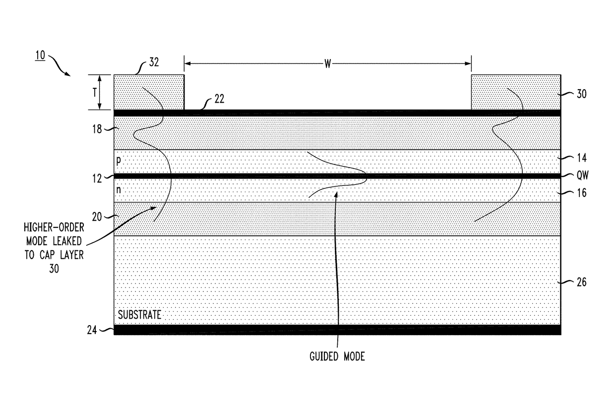
[0017]The present invention relates to a broad area laser structure that overcomes problems associated with thermal lensing (i.e., the presence of a thermally-induced waveguide) and provides a high power, broad area laser with fewer supported laser modes and, therefore, a smaller lateral farfield than various prior art configurations. In accordance with the present invention, an anti-guiding layer of a material with a refractive index higher than that associated with desired mode is formed outside of the primary waveguide of the laser structure. The presence of this high refractive index anti-guiding layer, as explained below, optically “pulls” the undesired higher-order lateral modes out of the active region of the laser and into a region where they can “leak” out of the device and no longer impede its performance.

[0018]FIG. 1 illustrates the principles of the present invention, in this case based upon the use of an inverted ridge broad area laser design. A broad area laser 10 is s...


PUM


Abstract

A broad area laser diode is configured to include an anti-guiding layer located outside of the active region of the device. The anti-guiding layer is formed of a high refractive index material that serves to de-couple unwanted, higher-order lateral modes (attributed to thermal lensing problems) from the lower-order mode output beam of output signal from the laser diode. The anti-guiding layer is formed using a single epitaxial growth step either prior to or subsequent to the steps used to grow the epitaxial layers forming the laser diode itself, thus creating a structure that provides suppression of unwanted higher-order modes without requiring a modification of specific process steps used to fabricate the laser diode itself.

Description

CROSS-REFERENCE TO RELATED APPLICATIONS[0001]This application claims the benefit of U.S. Provisional Application Ser. No. 62 / 180,766, filed Jun. 17, 2015 and herein incorporated by reference.TECHNICAL FIELD[0002]The present invention relates to a broad area laser diode and, more particularly, to a broad area laser diode including at least one anti-guiding layer disposed outside the active region of the laser diode to de-couple unwanted higher-order lateral modes and minimize lateral divergence in the farfield.BACKGROUND OF THE INVENTION[0003]In broad area lasers, the lateral divergence of the emitted radiation increases with increasing output power, as a result of the increase in thermal energy within the structure at higher powers. The laser is heated partly by the current flow into the laser, and partly by the re-absorption of the emitted light. Since the semiconductor materials utilized in the laser structure exhibit temperature-dependent refractive indices, a thermally-induced w...

Claims


Application Information

Patent Timeline
Patent Type & Authority Patents(United States)
IPC IPC(8): H01S5/00H01S5/22H01S5/24H01S5/34H01S5/20
CPCH01S5/205H01S5/2022H01S5/2031H01S5/2036H01S5/2202H01S5/24H01S5/34H01S5/22H01S2301/18
Inventor TELKKALA, JARKKOMULLER, JURGENLICHTENSTEIN, NORBERT
Owner II VI DELAWARE INC
Why Eureka
Try Eureka