Electronic device casing including coupling structure and method of manufacturing same

a technology of electronic devices and casings, which is applied in the direction of casings/cabinets/drawers, casings/cabinets/drawers details, manufacturing tools, etc., can solve the problems of long manufacturing time, complex manufacturing process of casings, and consumers' impression of inferior quality

Inactive Publication Date: 2017-10-24
SUNTENG NEW TECH
View PDF14 Cites 6 Cited by
  • Summary
  • Abstract
  • Description
  • Claims
  • Application Information

AI Technical Summary

Benefits of technology

[0013]In the method for manufacturing an electronic device casing including a coupling structure of the present invention, the preliminary connecting section is formed on the first thermoplastic substrate by the hot-pressing molding process, and the molding plastic material is then injected onto the preliminary connecting section by the in-mold injection process. After being cooled, the molding plastic material engages with the preliminary connecting section to form the secondary connecting section, such that the coupling structure is formed. Thus, the coupling structure can be directly formed during the manufacturing process of the electronic device casing without any additional procedures. Therefore, the coupling structure provided by the present invention is suitable for mass production due to a simplified manufacturing process and shortened manufacturing time.

Problems solved by technology

Although having advantages of being light in weight and high in formability, plastics suffer from an issue of unsatisfactory heat dissipation and are also likely to leave consumers an impression of an inferior quality.
However, a coupling structure cannot be directly formed on the casing made of metal for coupling with an external element (e.g., a circuit board or a bracket).
In the above disclosures, although an issue of not being able to directly form a coupling structure is solved, adhesion or welding of the coupling structure requires extremely precise positioning to ensure that an external element can be steadily coupled with the casing, which makes the manufacturing process of the casing complex and lengthens manufacturing time thereof.

Method used


Image

  • Electronic device casing including coupling structure and method of manufacturing same
  • Electronic device casing including coupling structure and method of manufacturing same
  • Electronic device casing including coupling structure and method of manufacturing same

Examples


Embodiment Construction

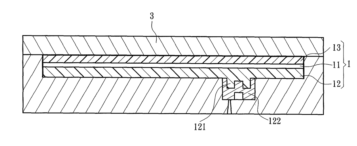
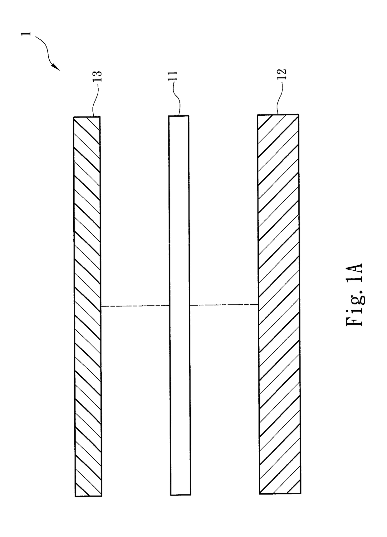
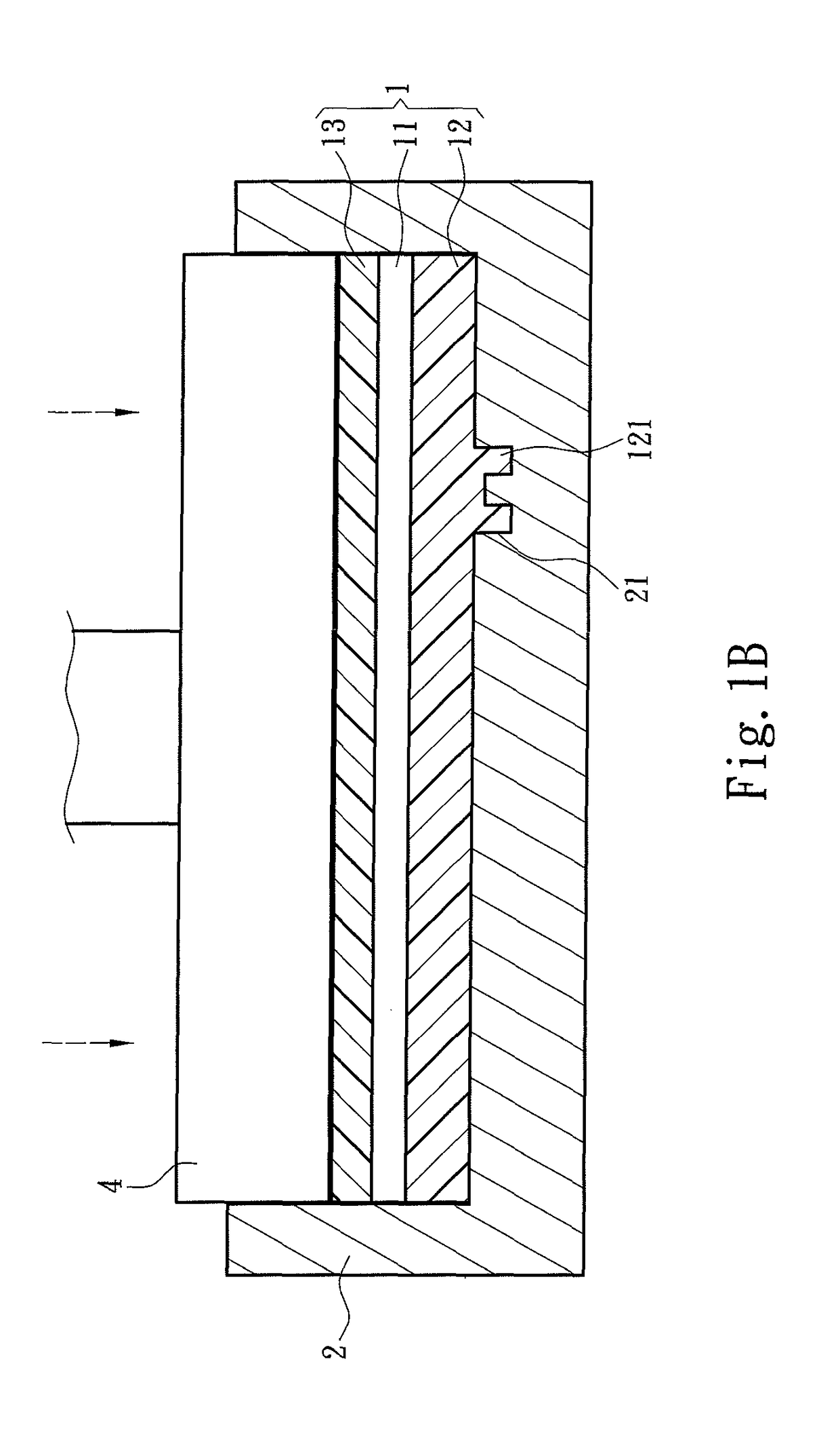
[0022]Referring to FIG. 1A and FIG. 2, an electronic device casing including a coupling structure according to an embodiment of the present invention is used for coupling with a circuit board (not shown) or a bracket (not shown) of an electronic device. The coupling structure is directly disposed on a surface of the electronic device casing, and so an issue of a conventional coupling structure disposed on the electronic device casing through welding or adhesion can be solved. The electronic device casing is made of a casing material 1. The casing material 1 comprises a supportive substrate 11, and a first thermoplastic substrate 12 stacked on a surface of the supportive substrate 11. The supportive substrate 11 may be made of a material selected from the group consisting of metal, fiber and carbon fiber. The first thermoplastic substrate 12 may be made of a material selected from the group consisting of polyethylene terephthalate (PET), polyethylene naphthalate (PEN), polyethylene g...


PUM

PropertyMeasurementUnit
thicknessaaaaaaaaaa
thicknessaaaaaaaaaa
thicknessaaaaaaaaaa

Abstract

A method for manufacturing an electronic device casing having a coupling structure is provided. The electronic device casing is made of a casing material including a supportive substrate and a first thermoplastic substrate. A preliminary connecting section is formed on the first thermoplastic substrate by a hot-pressing molding process, and a molding plastic material is injected onto the preliminary connecting section by an in-mold injection process. After being cooled, the molding plastic material engages with the preliminary connecting section to form a secondary connecting section for a coupling element to couple with. Thus, the coupling structure of the electronic device casing can be directly formed during a manufacturing process without any additional procedures, thereby overall manufacturing time and costs are reduced.

Description

FIELD OF THE INVENTION[0001]The present invention relates to an electronic device casing including a coupling structure and a method of manufacturing same, and particularly to a method for manufacturing an electronic device casing including a coupling structure which is formed on a first thermoplastic substrate by a hot-pressing molding process in conjunction with an in-mold injection process.BACKGROUND OF THE INVENTION[0002]To stimulate purchase desires of consumers, in addition to pursuing outstanding function performance, manufacturers of industrial products provide the products in diversified novel appearance designs that are not only appealing to consumers but also enhance added values of the products. Taking a casing of an electronic device as an example, casings in earlier days are commonly made of plastic materials through an injection molding process. Although having advantages of being light in weight and high in formability, plastics suffer from an issue of unsatisfactory...

Claims


Application Information

Patent Timeline
Patent Type & Authority Patents(United States)
IPC IPC(8): B28B3/20H05K5/00B29C45/14B29C69/02H05K5/02B29C43/18B29C70/84B29C43/20B29L31/34
CPCH05K5/0217B29C45/14336B29C69/02H05K5/0034Y10T428/249923B29C43/183B29C43/20B29L2031/3481
Inventor WANG, WEN-CHENG
Owner SUNTENG NEW TECH
Why Eureka
Try Eureka