Optical backplane mirror

a backplane mirror and optical technology, applied in the field of optical backplane mirrors and fabrication of optical interface structures, can solve the problems of reducing coupling efficiency, transmission failure, and integrating optical interconnects

Active Publication Date: 2017-11-07
NXP USA INC
View PDF126 Cites 3 Cited by
  • Summary
  • Abstract
  • Description
  • Claims
  • Application Information

AI Technical Summary

Problems solved by technology

But in addition to the difficulty of integrating optical communication systems within IC chips, there are challenges associated with integrating optical interconnects between IC chips.
Even so, there remain many technical challenges to realizing efficient optical coupling between optical communication systems at each IC chip, including reducing positional or signal alignment inaccuracies in the optical path (that can decrease the coupling efficiency or lead to transmission failure), accounting for perpendicular alignment between an IC chip relative to the backplane interconnect, and the fabrication costs and complexities associated with forming optical interconnects (e.g., active optoelectronic devices) that are capable of coupling optical signals between IC chips.
Attempts have been made to overcome these challenges by using fiber optic waveguides and / or external mirrors or deflectors in the printed circuit board or off chip to optically transfer information between different IC chips, but these solutions present their own difficulties, costs, and control requirements.
For example, fiber optic waveguides not only have additional costs and complexity, but may also impose bandwidth limitations on chip-to-chip communications.
In addition, the cost for designing and assembling the optical transmitter, external mirrors or deflectors, and the optical receiver, as well as the requirements for achieving alignment with these components to ensure a desired level of information transmission, may be cost prohibitive.
Finally, control circuits and external signal deflection structures can increase the overall system complexity, thereby reducing possible signal bandwidth between different IC chips.
As a result, the existing solutions for interconnecting optical communication systems from different IC chips make the implementation of high bandwidth optical interconnects extremely difficult at a practical level.

Method used


Image

  • Optical backplane mirror
  • Optical backplane mirror
  • Optical backplane mirror

Examples


Embodiment Construction

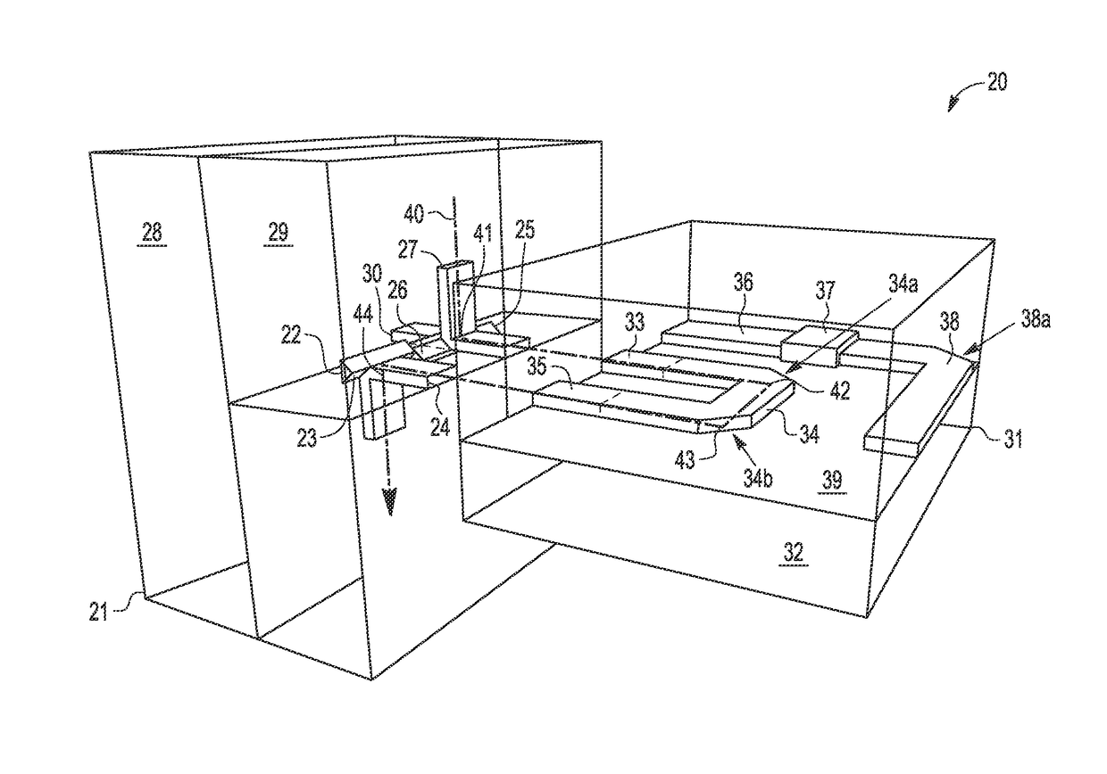
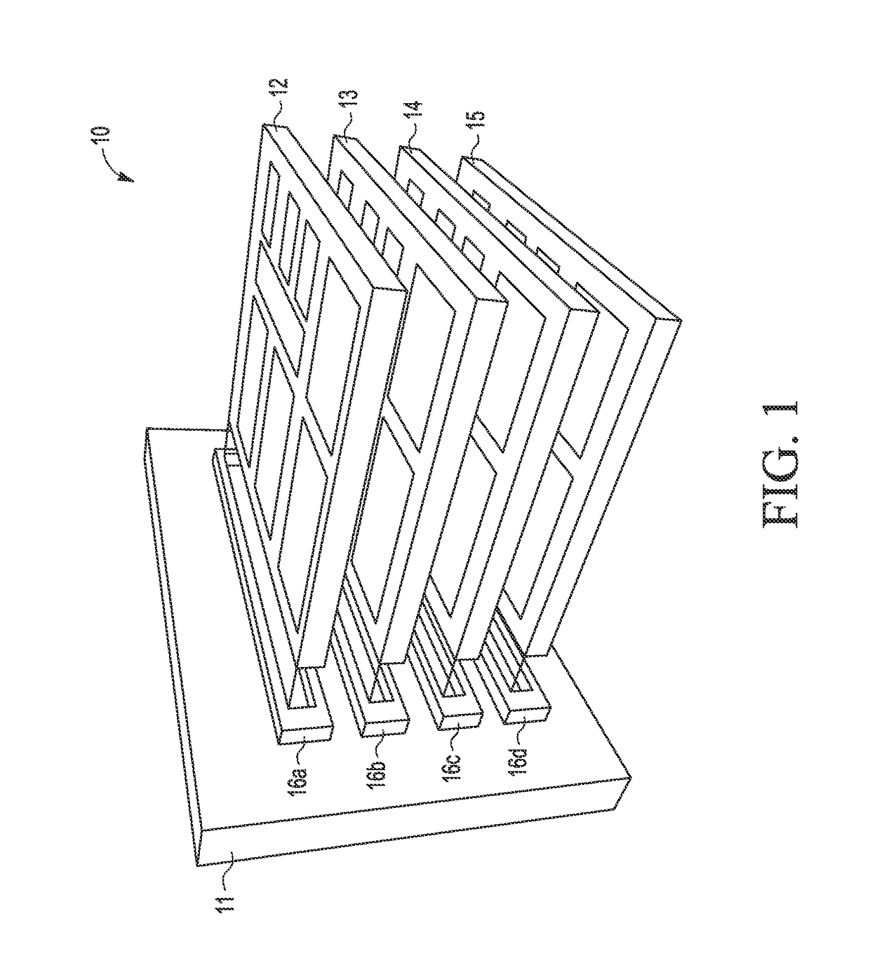
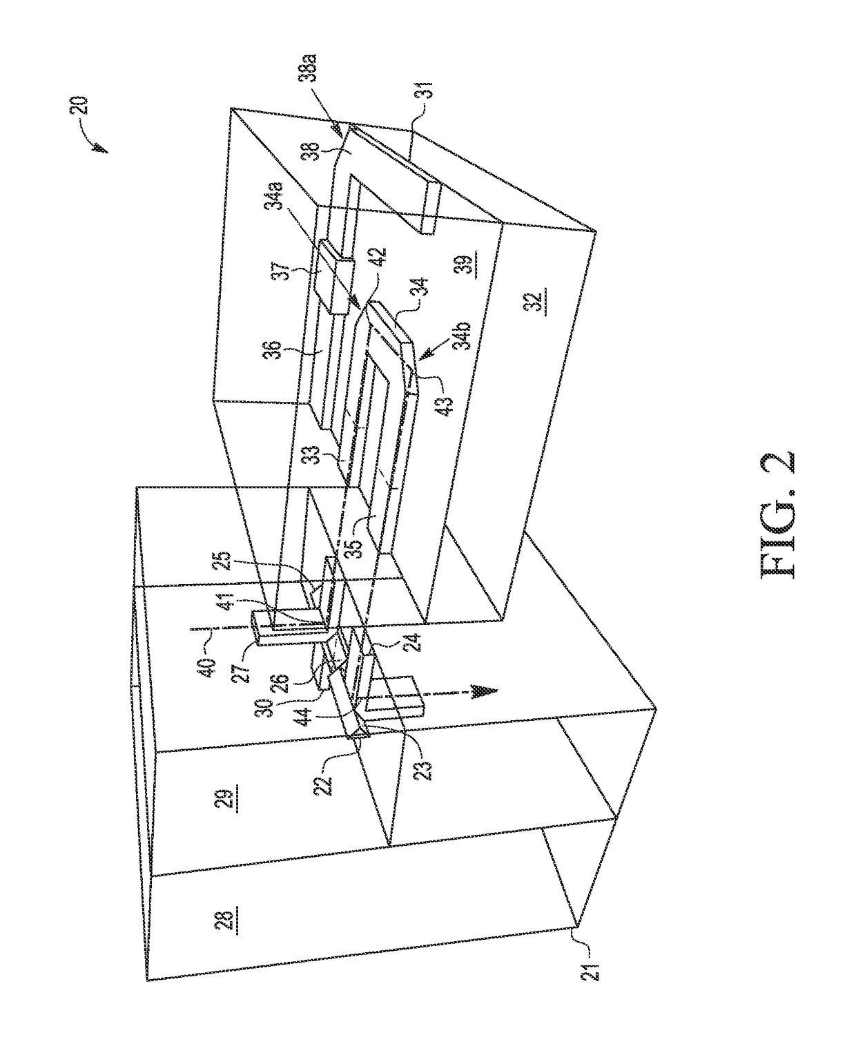
[0019]There are disclosed herein improved optical communication systems, methods, and apparatus that address various problems in the art where various limitations and disadvantages of conventional solutions and technologies will become apparent to one of skill in the art after reviewing the remainder of the present application with reference to the drawings and detailed description provided herein. In selected embodiments, a high density, low power, high performance information system, method and apparatus are described in which integrated optical communications are provided by forming an integrated circuit die with optical mirror structures to move optical signals through and around one or more integrated circuit die mounted or communicating with the integrated circuit die. In embodiments where one or more vertical die or die stacks are mounted on an optical backplane die, optical connections between different die are providing by using bulk silicon micromachining technology to fab...


PUM


Abstract

An integrated circuit optical backplane die and associated semiconductor fabrication process are described for forming optical backplane mirror structures for perpendicularly deflecting optical signals out of the plane of the optical backplane die by selectively etching an optical waveguide semiconductor layer (103) on an optical backplane die wafer using an orientation-dependent anisotropic wet etch process to form a first recess opening (107) with angled semiconductor sidewall surfaces (106) on the optical waveguide semiconductor layer, where the angled semiconductor sidewall surfaces (106) are processed to form an optical backplane mirror (116) for perpendicularly deflecting optical signals to and from a lateral plane of the optical waveguide semiconductor layer.

Description

CROSS-REFERENCE TO RELATED APPLICATIONS[0001]U.S. patent application Ser. No. 13 / 913,993, entitled “Optical Wafer and Die Probe Testing,” by inventors Michael B. McShane, Perry H. Pelley, and Tab A. Stephens, filed herewith Jun. 10, 2013, describes exemplary methods and systems and is incorporated by reference in its entirety.[0002]U.S. patent application Ser. No. 13 / 914,021, entitled “Die Stack with Optical TSVS,” by inventors Perry H. Pelley, Tab A. Stephens, and Michael B. McShane, filed herewith Jun. 10, 2013, describes exemplary methods and systems and is incorporated by reference in its entirety.[0003]U.S. patent application Ser. No. 13 / 914,049, entitled “Communication System Die Stack,” by inventors Tab A. Stephens, Perry H. Pelley, and Michael B. McShane, filed herewith Jun. 10, 2013, describes exemplary methods and systems and is incorporated by reference in its entirety.[0004]U.S. patent application Ser. No. 13 / 914,089, entitled “Integration of a MEMS Beam with Optical Wav...

Claims


Application Information

Patent Timeline
Patent Type & Authority Patents(United States)
IPC IPC(8): G02B6/12G02B6/136G02B6/13G02B6/125G02B6/43G02B6/42
CPCG02B6/136G02B6/125G02B6/131G02B6/43G02B2006/12104G02B6/4214G02B2006/12061
Inventor STEPHENS, TAB A.PELLEY, PERRY H.MCSHANE, MICHAEL B.
Owner NXP USA INC
Why Eureka
Try Eureka