Eureka AIR delivers breakthrough ideas for toughest innovation challenges, trusted by R&D personnel around the world.

Efuse bit cell, and read/write method thereof, and efuse array

a bit cell and array technology, applied in the field of efuse bit cells and read/write methods thereof, and efuse arrays, can solve the problems of low integration level of srams, direct affecting user experience, and inability to save data

Active Publication Date: 2017-11-28
SEMICON MFG INT (SHANGHAI) CORP +1
View PDF5 Cites 8 Cited by
  • Summary
  • Abstract
  • Description
  • Claims
  • Application Information

AI Technical Summary

Benefits of technology

[0010]Another aspect of the present disclosure includes a read / write method of an Efuse bit cell. The method includes providing an Efuse bit cell, including a data latch having two branches with a fuse disposed in a first branch and a resistor disposed in a second branch, two terminals of the fuse being configured as a first latching node and a second latching node, respectively, two terminals of the resistor being configured as a third latching node and a fourth latching node, respectively, the second latching node being connected to the second branch and the fourth latching node being connected to the first branch; a selection controller configured to control connections between one terminal of the first branch and a power source and between one terminal of the second branch and the power source, another terminal of the first branch and another terminal of the second branch being connected to ground; a first diode and a second diode, one of the first diode and the second diode being configured to input a write data signal; and a pass unit configured to transmit data stored in the Efuse bit cell and output a bit line signal; turning on the selection controller to control connections between the first branch and the power source and between the second branch and the power source; turning on the pass unit to transmit data stored in the Efuse cell bit and output bit line signals, turning off the selection controller, turning off the pass unit; and programming the fuse.
[0056]Therefore, when the integrated chip having the disclosed Efuse bit cell is first powered-on, the data stored in the fuse included in the Efuse bit cell may be read. Because the pass unit may be controlled by the word line signal, the word line signal may be synchronized with the system clock of the integrated chip. Accordingly, the data reading of the fuse included in the Efuse bit cell may also be synchronized with the system clock of the chip. Thus, the system powering-up time of the chip may be improved.
[0058]Further, the output signals BL and \BL of the existing 6T SRAM may be directly connected to two corresponding latching nodes, which is sensitive to DC noises; and is easy to invert the latching status of the latching points. Thus, the anti-interference ability may not be acceptable. The pass unit of the disclosed Efuse bit cell may include a third NMOS transistor and a fourth NMOS transistor. When the data latched in the Efuse bit unit is read, the effect of the bit line signals at the output terminal of the fourth NMOS transistor to the fourth latching node may be effectively avoided, and the inversion of the latching data may be avoided. Thus, the read disturb may be avoided.
[0011]Another aspect of the present disclosure includes an Efuse array. The Efuse array includes at least two parallel row lines and at least two parallel column lines forming a plurality of nodes, each node corresponding to an Efuse bit cell; a selection controller configured to control connections between one terminal of the first branch and a power source and between one terminal of the second branch and the power source, another terminal of the first branch and another terminal of the second branch being connected to ground; a first diode and a second diode, one of the first diode and the second diode being configured to input write data signals; and a pass unit configured to transmit data stored in the Efuse bit cell and output bit line signals; a plurality of row selectors configured to input address signals, each row selector being controlled on / off and each row selector being connected to one of the at least two row lines; and a plurality of column selectors configured to input address signals, each column selector being controlled on / off and each row selector being connected to one of the at least two column lines. The Efuse bit cell includes a data latch having two branches with a fuse disposed in a first branch and a resistor disposed in a second branch, two terminals of the fuse being configured as a first latching node and a second latching node, respectively, two terminals of the resistor being configured as a third latching node and a fourth latching node, respectively, the second latching node being connected to the second branch and the fourth latching node being connected to the first branch.

Problems solved by technology

However, the integration level of SRAMs is low; and cannot save data when the power is off.
Thus, the system powering-up time of the chips directly affects the powering-up time of the cell phones and the laptop computers, and directly affects the user experience.
Such a large size causes the drain-gate load of the NMOS transistor to be relatively large; and its charging / discharging speed is relatively slow.
Such a relatively slow switching speed causes the NMOS transistor M11 to be unable to synchronize with the system clock; and increases the system powering-up time.
Thus, when the integrated chip having the Efuse IP core and the SRAM IP core is first powered-on, because the data reading by the SRAM IP core of the data stored in the Efuse IP core is unable to synchronize with the system clock, the system powering-up time is relatively long.
Further, the MOS transistors in the chip take up relatively large areas.

Method used


Image

  • Efuse bit cell, and read/write method thereof, and efuse array
  • Efuse bit cell, and read/write method thereof, and efuse array
  • Efuse bit cell, and read/write method thereof, and efuse array

Examples


Embodiment Construction

[0021]Reference will now be made in detail to exemplary embodiments of the invention, which are illustrated in the accompanying drawings. Wherever possible, the same reference numbers will be used throughout the drawings to refer to the same or like parts.

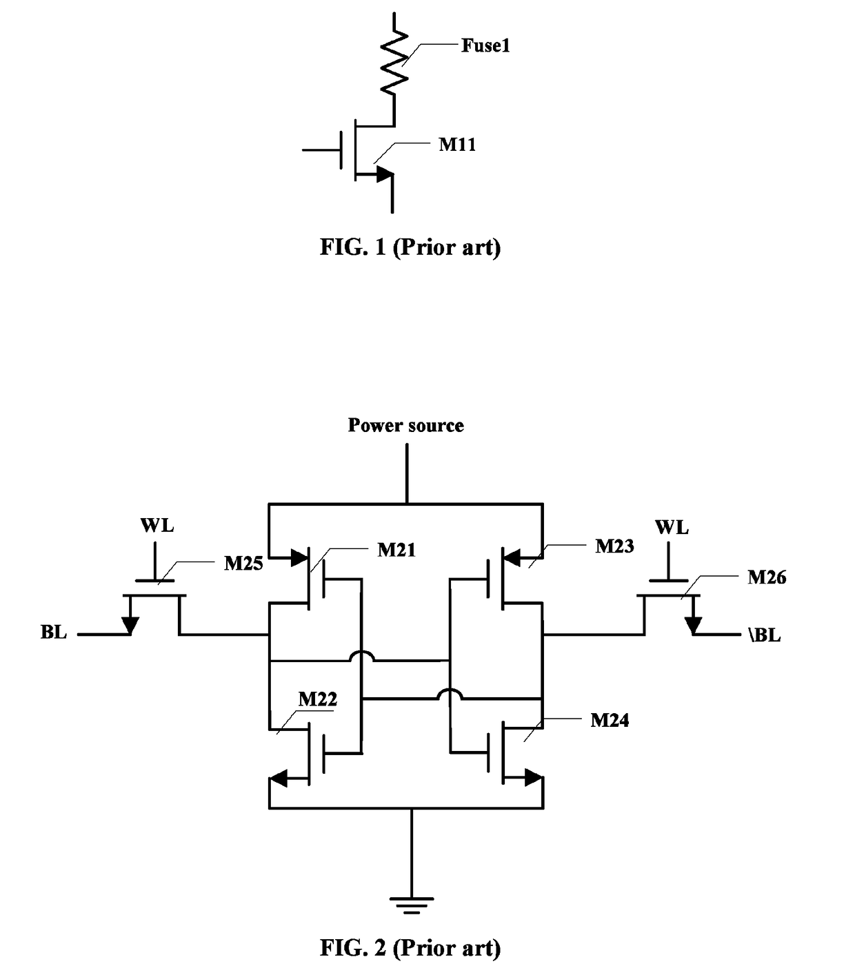
[0022]As described previously, when the integrated chip having the Efuse IP core and the SLAM IP core is first powered-on, because the data reading of by SRAM IP core of the data stored in the Efuse IP core is unable to synchronize with the system clock, the powering-up time is relatively long. Further, the MOS transistors in the chip take up relatively large areas, the area of the Efuse IP core is relatively large. Further, the existing 6T SRAMs are easy to be affected by DC noises. Thus, the anti-interference ability of the existing 6T SRAMs is relatively low.

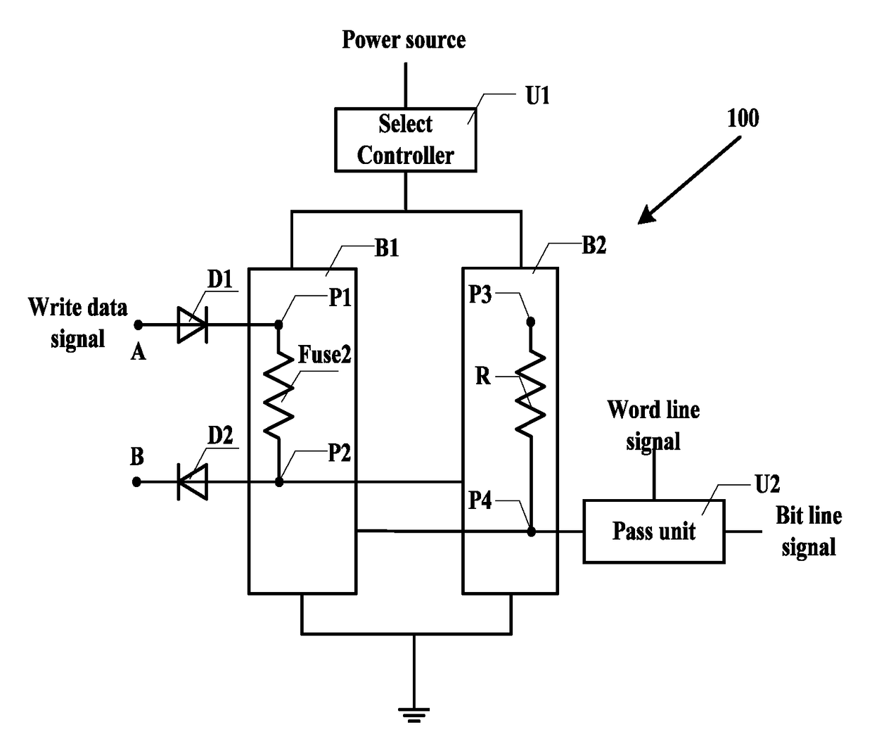
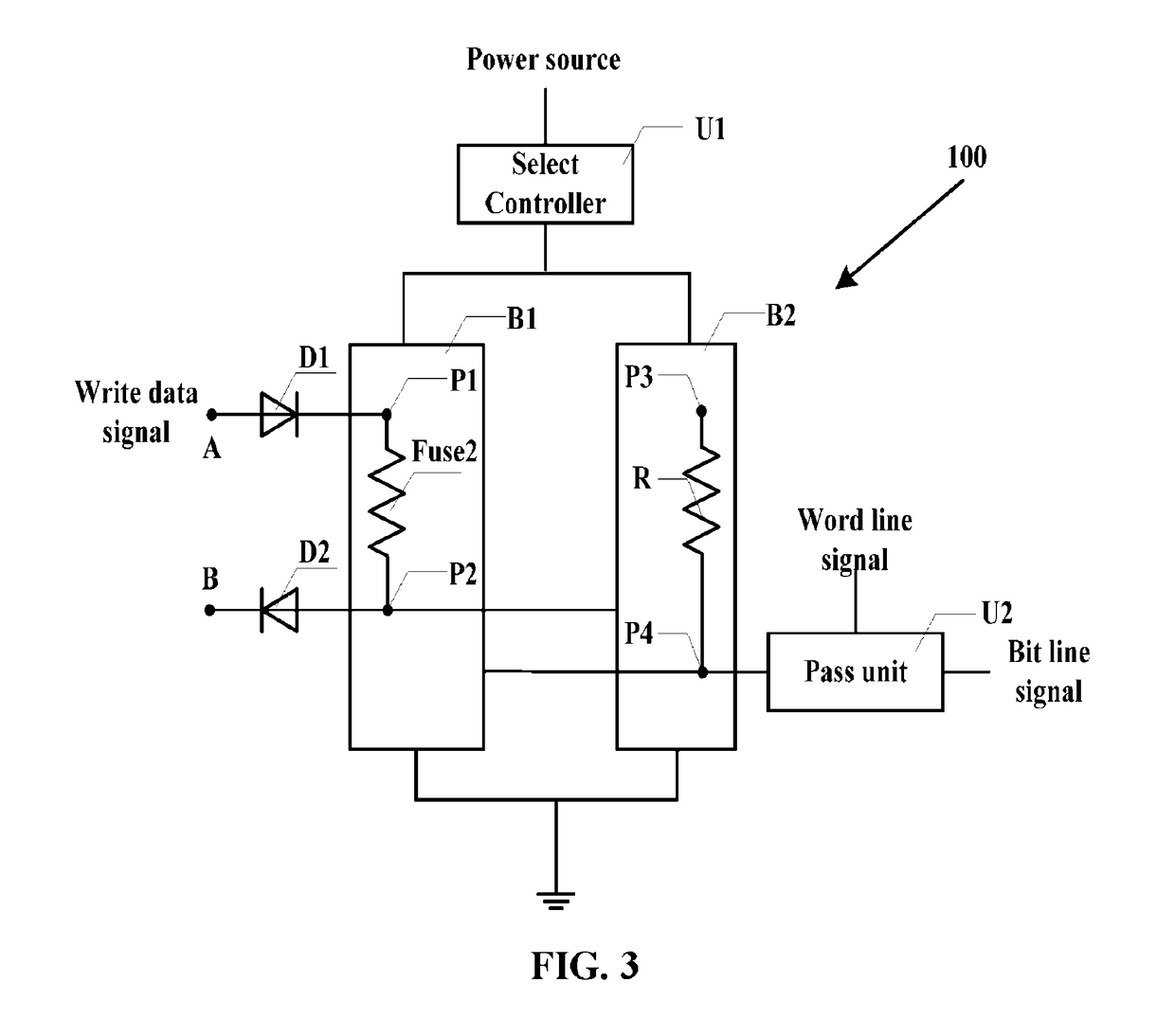
[0023]The present disclosure provides Efuse bit cells and read / write methods thereof, and Efuse arrays. FIG. 3 illustrates an exemplary Efuse bit cell consistent with the di...


PUM


Abstract

The present disclosure provides Efuse bit cells and read / write methods thereof, and Efuse arrays. An exemplary Efuse bit cell includes a data latch configured to latch data of the Efuse bit cell, having two branches with a fuse disposed in a first branch and a resistor disposed in a second branch; a selection controller configured to control connections between one terminal of the first branch and a power source and between one terminal of the second branch and the power source, another terminal of the first branch and another terminal of the second branch being connected to ground; a first diode and a second diode, one of the first diode and the second diode being configured to input a write data signal; and a pass unit configured to transmit data stored in the Efuse bit cell and output a bit line signal.

Description

CROSS-REFERENCES TO RELATED APPLICATIONS[0001]This application claims the priority of Chinese patent application No 201510707364.8, filed on Oct. 27, 2015, the entirety of which is incorporated herein by reference.FIELD OF THE INVENTION[0002]The present invention generally relates to the field of semiconductor circuit design technology and, more particularly, relates to Efuse bit cells and read / write methods thereof, and Efuse arrays.BACKGROUND[0003]Efuses, as a type of one time program (OTP) devices, may be programmed to store data. Static random access memories (SRAMs) are one of the common types of memory, which utilize a static access method, and use bistable data latching circuits as memory cells. SRAMs have a high read speed. The efficiency of SRAMs can be increased without cooperating with the memory refreshing circuits. However, the integration level of SRAMs is low; and cannot save data when the power is off. When an integrated chip having an Efuse intellectual property (IP...

Claims


Application Information

Patent Timeline
Patent Type & Authority Patents(United States)
IPC IPC(8): G11C17/00G11C17/18G11C17/16
CPCG11C17/165G11C17/18G11C14/0054G11C17/16
Inventor YANG, CHIA CHI
Owner SEMICON MFG INT (SHANGHAI) CORP
Why Eureka
Eureka Blog
Learn More