Artificial skin and elastic strain sensor

a technology of elastic strain and elastic skin, applied in the field of elastic strain and pressure sensors, can solve problems such as complex mechanical properties of pressure sensing

Active Publication Date: 2017-12-12
PRESIDENT & FELLOWS OF HARVARD COLLEGE
View PDF65 Cites 26 Cited by
  • Summary
  • Abstract
  • Description
  • Claims
  • Application Information

AI Technical Summary

Benefits of technology

[0041]Each of the microchannels 110 can be formed with a uniform cross-section and filled with the conducting liquid, such as eutectic gallium-indium (eGaIn) available from BASF, Florham Park, N.J. Each of the microchannels 110 can be substantially straight, zig-zag, or S shaped. In accordance with one embodiment, the microchannels 110 can be connected end to end by the loop portions 120 such that a single continuous channel filled with the conducting liquid 130 can be formed. In this embodiment, each microchannel extends parallel to the strain axis and when the elastic material is subject to strain, each of the microchannels, along with the conductive liquid 130 carried therein, can become elongated increasing the electrical resistance. One advantage of the present invention is that each microchannel becomes elongated causing the overall length of the channel of conducting liquid to be elongated in per portion to the number of microchannels. Adding microchannels can be used to increase the sensitivity of the strain sensor. In some embodiments, the sensor can include 36 or more microchannels 110, and each microchannel 110 can be 250 μm wide by 250 μm high and the loop portions can be 1.0 mm wide by 250 μm high.
[0042]Each of the microchannels 110 can be connected by loop portions 120 that forms a continuous channel that serpentines over a surface. In accordance with some embodiments of the invention, the loop portions 120 can be substantially larger in cross-sectional area than the unstrained microchannels 110 such that strain in a direction transverse to the strain axis 104 does not cause significant change in electrical resistance. In this embodiment, the elastic stain sensor 100 becomes unidirectional along the strain axis 104.
[0043]The elastic strain sensor 100 can be formed from any elastic material including silicone and rubber materials (e.g., EcoFlex0030 and EcoFlex0050, SmoothOn, Easton, Pa.; PDMS, Dow Corning, Midland, Mich.; P-20 and GI-1120, Innovative Polymers, Saint Johns, Mich.; Tap Platinum Silicone System, Tap Plastics, CA) and soft polyurethane materials (e.g., Dragon Skin, SmoothOn, Easton, Pa.; IE-35A, Innovative Polymers, Saint Johns, Mich.). In accordance with one embodiment, a low viscosity (3000 cps) mixture of EcoFlex can be used to reproduce the fine features of the mold.
[0044]In general, the process for fabricating the sensor can include mold making, casting the layer(s), bonding the layers together and injecting the conducting liquid. In accordance with one embodiment of the invention, the elastic strain sensor 100 can be produced by casting the silicone material into one or more 3D printed molds (e.g., Connex 500, Objet Geometries Ltd.). In this embodiment, one layer can be patterned to form the microchannels 110, loop portions 120 and connection reservoirs 132, 134 and the other layer is not patterned, providing an essentially flat layer to be bonded to the patterned layer. After curing under ambient conditions for approximately 4 h, the elastomer layers can be removed from the molds and bonded together with a thin, uncured layer of the elastomer material (e.g., EcoFlex).
[0045]To avoid filling the exposed microchannels, the unpatterned elastomer mold can be first spin-coated with a thin, uncured layer (e.g., 1100 rpm for 45 s) of elastomer, which can be then partially cured, for example, for 30 s at 60° C. in a convection oven. The patterned elastomer mold can then be gently bonded to the unpatterned surface. The two elastomer layers (the unpatterned smooth sheet and the patterned sheet containing the exposed microchannels) can be cured together under ambient conditions for several hours. After the sheets are sufficiently bonded together, a syringe can be used to fill each channel with eGaIn. Lastly, the ends of the channel can be sealed with a final coating of uncured elastomer material.
[0046]In accordance with another embodiment of the invention, sensors with microchannels in the 20-300 micrometer range can be fabricated by casting an elastomer material (e.g., PDMS) in an SU-8 mold that is patterned by maskless soft lithography. Photoresist (SU-8 2050) can be spun onto a clean silicon wafer, for example, at 500 rpm for 10 s (spread), followed by 4000 rpm for 30 s (spin). The wafer can then be placed on a hot plate at 65° C. for 3 min and 95° C. for 6 min. Next, the coated wafer can be patterned via direct-write laser exposure [25, 26] using a diode pumped solid-state (DPSS) 355 nm laser micromachining system. The system can be calibrated to expose a 20 μm thick SU-8 coating to produce channels with a range of 25 to 1000 μm in width and >50 μm spacing. The wafer can be post-baked on a hot plate, for example, at 65° C. for 1 min and 95° C. for 6 min, and consequently developed for 5 min in SU-8 developer. In order to allow for easier removal in subsequent molding steps, a hydrophobic monolayer can be introduced through vapor deposition. The patterned wafer can be placed in an evacuated chamber (20 mTorr) with an open vessel containing a few drops of trichloro (1H,1H,2H,2H-perfluorooctyl) silane (Aldrich) for 3 h. Next, the PDMS (Sylgard 184; Dow Corning, Midland, Mich.) can be cast in liquid form (e.g., 10:1 mass ratio of elastomer base to curing agent) against the silicon wafer. PDMS can then be partially cross-linked in the mold by oven-curing at 60° C. for 30-40 min. The microchannels can be constructed by bonding patterned PDMS to unpatterned PDMS via oxygen plasma treatment (Technics Plasma Stripper / Cleaner; 60 W for 30 s). The sealed microchannels can be completely cured, for example, at 60° C. overnight. Finally, the microchannels can be filled with eGaIn using conventional tubing and syringe dispensing.

Problems solved by technology

In contrast to strain sensing, the mechanics of pressure sensing are complex and involve the use of elasticity and contact mechanics to derive a predictive mathematical model for describing the relationship between external pressure and electrical conductivity.

Method used


Image

  • Artificial skin and elastic strain sensor
  • Artificial skin and elastic strain sensor
  • Artificial skin and elastic strain sensor

Examples


Embodiment Construction

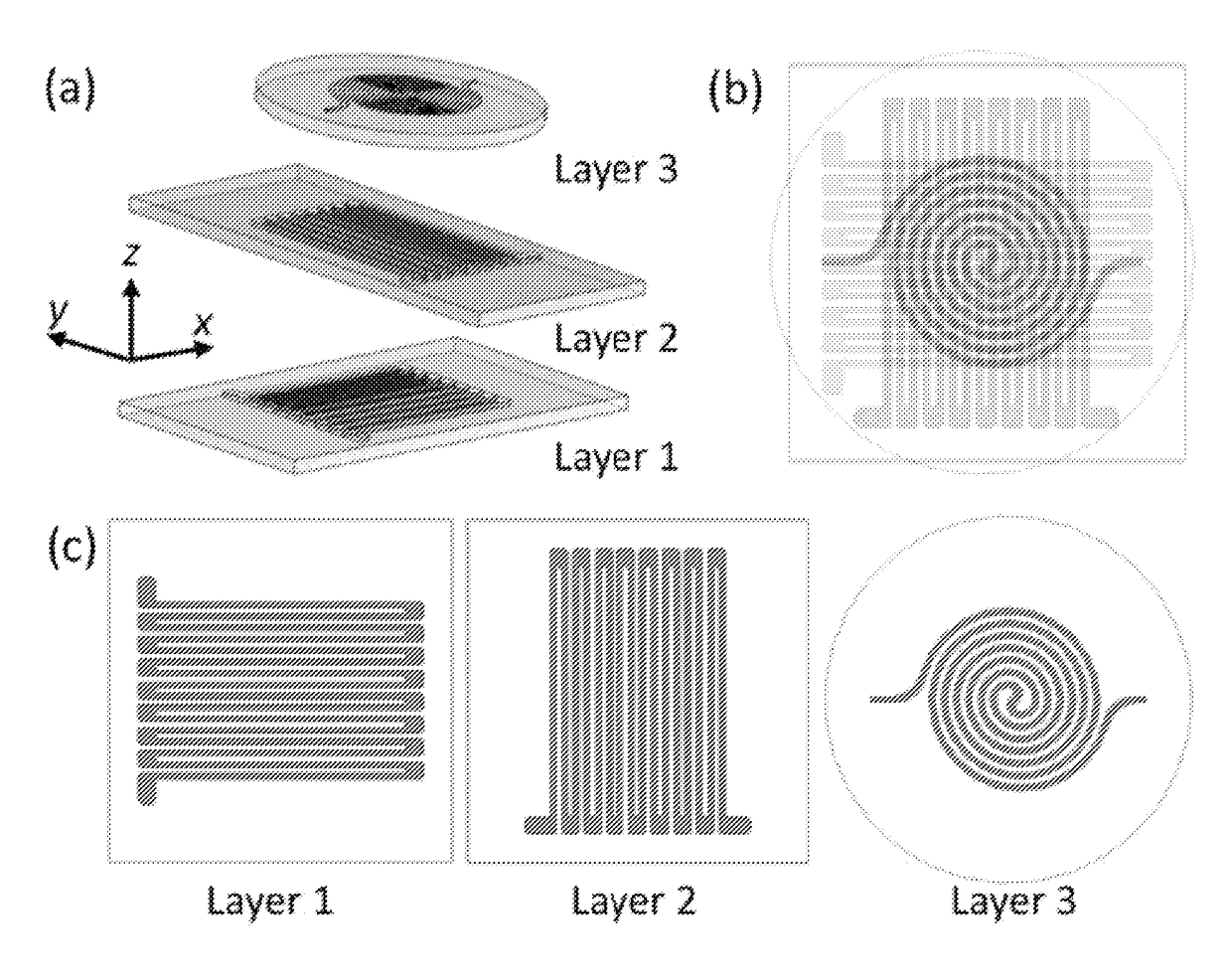
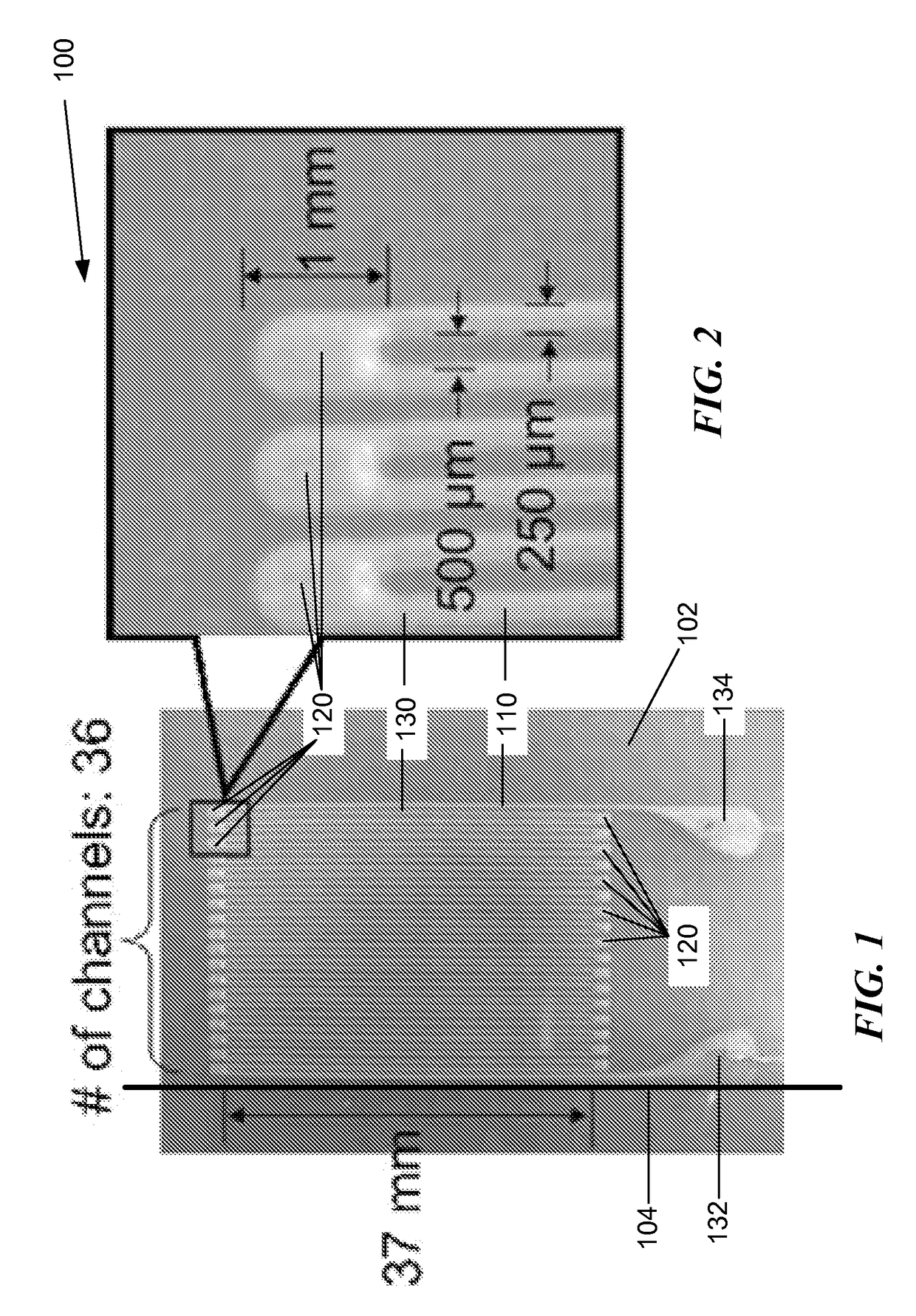
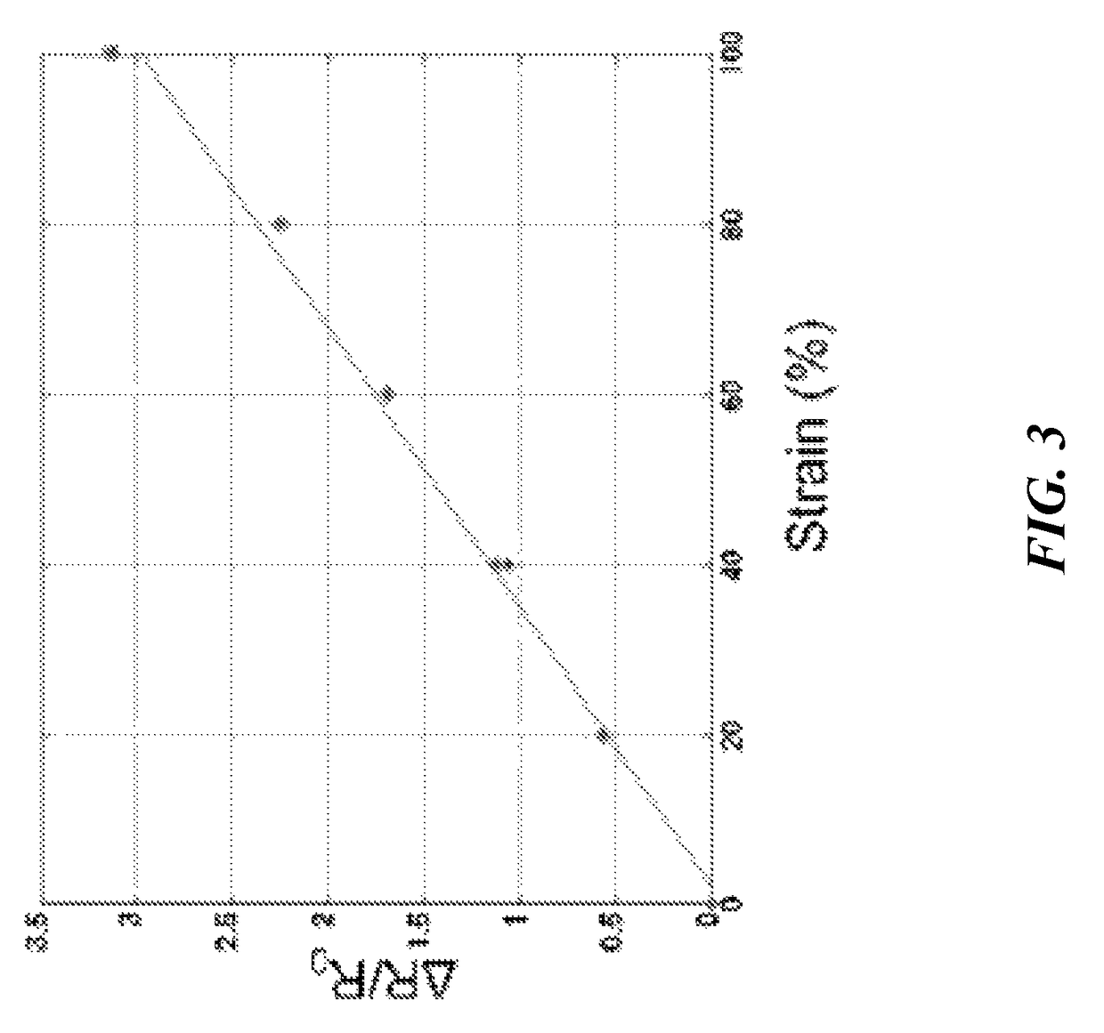
[0038]The present invention is directed to elastic sensors and methods for fabricating elastic sensors that respond to strain in a single direction. This can be accomplished by forming a set of elongated microchannels in an elastic material such as silicone rubber sheet (EcoFlex 0030, SmoothOn, Easton, Pa.; PDMS, Dow Corning). Each microchannel can be formed to extend substantially parallel to a strain axis and the microchannels can be interconnected at their ends by loop portions to form a continuous channel over which to measure electrical resistance. The continuous channel can be filled with a conductive material, such as a conductive liquid, for example, non-toxic eutectic gallium-indium (eGaIn, BASF). In accordance with some embodiments of the invention, the loop portions can that have sufficient cross-sectional area in a direction transverse to the strain axis that strain in a direction transverse to the strain axis does not result in significant change in electrical resistanc...


PUM

PropertyMeasurementUnit
widthaaaaaaaaaa
widthaaaaaaaaaa
thickaaaaaaaaaa

Abstract

An elastic strain sensor can be incorporated into an artificial skin that can sense flexing by the underlying support structure of the skin to detect and track motion of the support structure. The uni-directional elastic strain sensor can be formed by filling two or more channels in an elastic substrate material with a conductive liquid. At the ends of the channels, a loop port connects the channels to form a serpentine channel. The channels extend along the direction of strain and the loop portions have sufficiently large cross-sectional area in the direction transverse to the direction of strain that the sensor is unidirectional. The resistance is measured at the ends of the serpentine channel and can be used to determine the strain on the sensor. Additional channels can be added to increase the sensitivity of the sensor. The sensors can be stacked on top of each other to increase the sensitivity of the sensor. In other embodiments, two sensors oriented in different directions can be stacked on top of each other and bonded together to form a bidirectional sensor. A third sensor formed by in the shape of a spiral or concentric rings can be stacked on top and used to sense contact or pressure, forming a three dimensional sensor. The three dimensional sensor can be incorporated into an artificial skin to provide advanced sensing.

Description

CROSS-REFERENCE TO RELATED APPLICATIONS[0001]This application is a 35 U.S.C. §371 National Phase Entry Application of International Application No. PCT / US2012 / 056903 filed Sep. 24, 2012, which designates the U.S., and which claims any and all benefits under law including benefit under 35 U.S.C. §119(e) of the U.S. Provisional Application No. 61 / 538,841, filed Sep. 24, 2011, the contents of each of which are incorporated herein by reference in their entirety.[0002]This application is related to U.S. Application Ser. No. 61 / 387,740, filed on Sep. 29, 2010, which is hereby incorporated by reference in its entirety.STATEMENT REGARDING FEDERALLY SPONSORED RESEARCH[0003]This invention was made with US government support under grant no. CNS 0932015 awarded by the National Science Foundation. The US government has certain rights in the invention.REFERENCE TO MICROFICHE APPENDIX[0004]Not ApplicableBACKGROUNDTechnical Field of the Invention[0005]The present invention is directed to elastic st...

Claims


Application Information

Patent Timeline
Patent Type & Authority Patents(United States)
IPC IPC(8): G01L1/22G06F3/01B25J13/08A61B5/103A43B23/02A43B13/20A61F2/10A61B5/11A61B5/00
CPCG01L1/22A43B13/203A43B23/029A61B5/1036A61B5/112A61F2/105G01L1/2287G06F3/011G06F3/014B25J13/08A61B2562/0261A61B5/6807A61B2562/0247
Inventor WOOD, ROBERT J.PARK, YONG-LAEMAJIDI, CARMEL S.CHEN, BOR-RONGSTIRLING, LEIAWALSH, CONOR JAMESNAGPAL, RADHIKAYOUNG, DIANAMENGUC, YIGIT
Owner PRESIDENT & FELLOWS OF HARVARD COLLEGE
Why Eureka
Try Eureka