High frequency circuit module in which high frequency circuits are embedded in a multilayer circuit substrate

a high frequency circuit and circuit substrate technology, applied in the field of high frequency circuit modules, can solve the problems of difficult to solve characteristic degradation problems, limit the possibility of further size reduction and thickness reduction, and achieve size and thickness reduction, etc., to achieve favorable high frequency characteristics, high shielding effect, and greater thickness

Active Publication Date: 2018-01-09
TAIYO YUDEN KK
View PDF15 Cites 6 Cited by
  • Summary
  • Abstract
  • Description
  • Claims
  • Application Information

AI Technical Summary

Benefits of technology

[0010]The present invention was made in view of the above situations, and an object thereof is to provide a high frequency circuit module that has excellent high frequency characteristics and that can achieve size reduction with ease.
[0022]A high frequency circuit module of the present invention as described above can achieve favorable high frequency characteristics and a reduction in size with ease.

Problems solved by technology

However, with conventional configurations of high frequency circuit modules, due to a problem of characteristic degradation caused by interference between signal lines or a stray capacitance between a signal line and a ground pattern, there were limits to further size reduction and reduction in thickness.
However, the technologies disclosed in Patent Documents 1 to 3 each has a structure contingent on a high frequency switch and filter being mounted on a surface of a circuit substrate, and thus merely embedding a high frequency switch or filter in these circuit substrates makes it difficult to solve problems of characteristic degradation (stray capacitance occurring in the high frequency switch and the periphery thereof, in particular), or to achieve a size and thickness reduction.

Method used


Image

  • High frequency circuit module in which high frequency circuits are embedded in a multilayer circuit substrate
  • High frequency circuit module in which high frequency circuits are embedded in a multilayer circuit substrate
  • High frequency circuit module in which high frequency circuits are embedded in a multilayer circuit substrate

Examples


embodiment 1

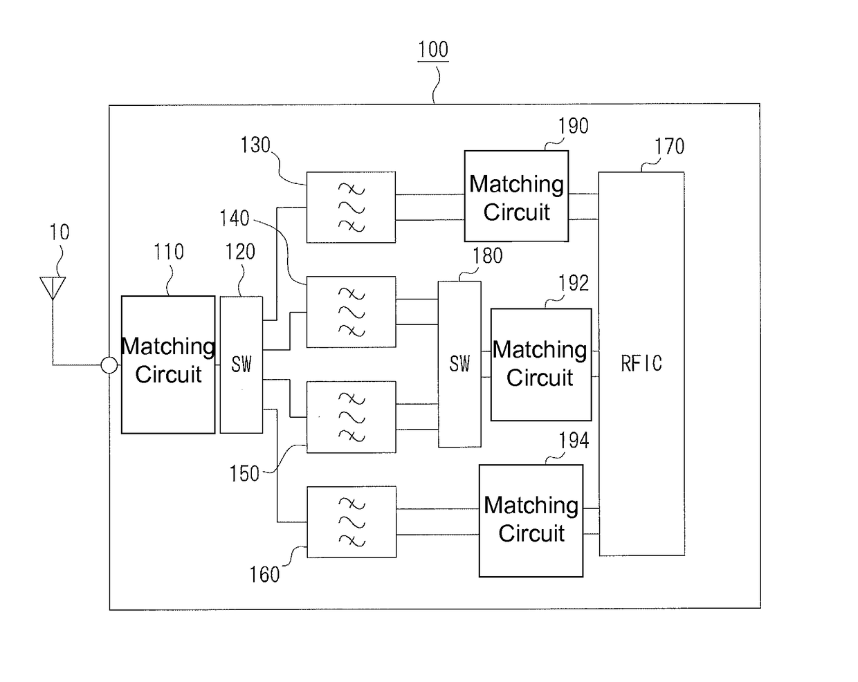
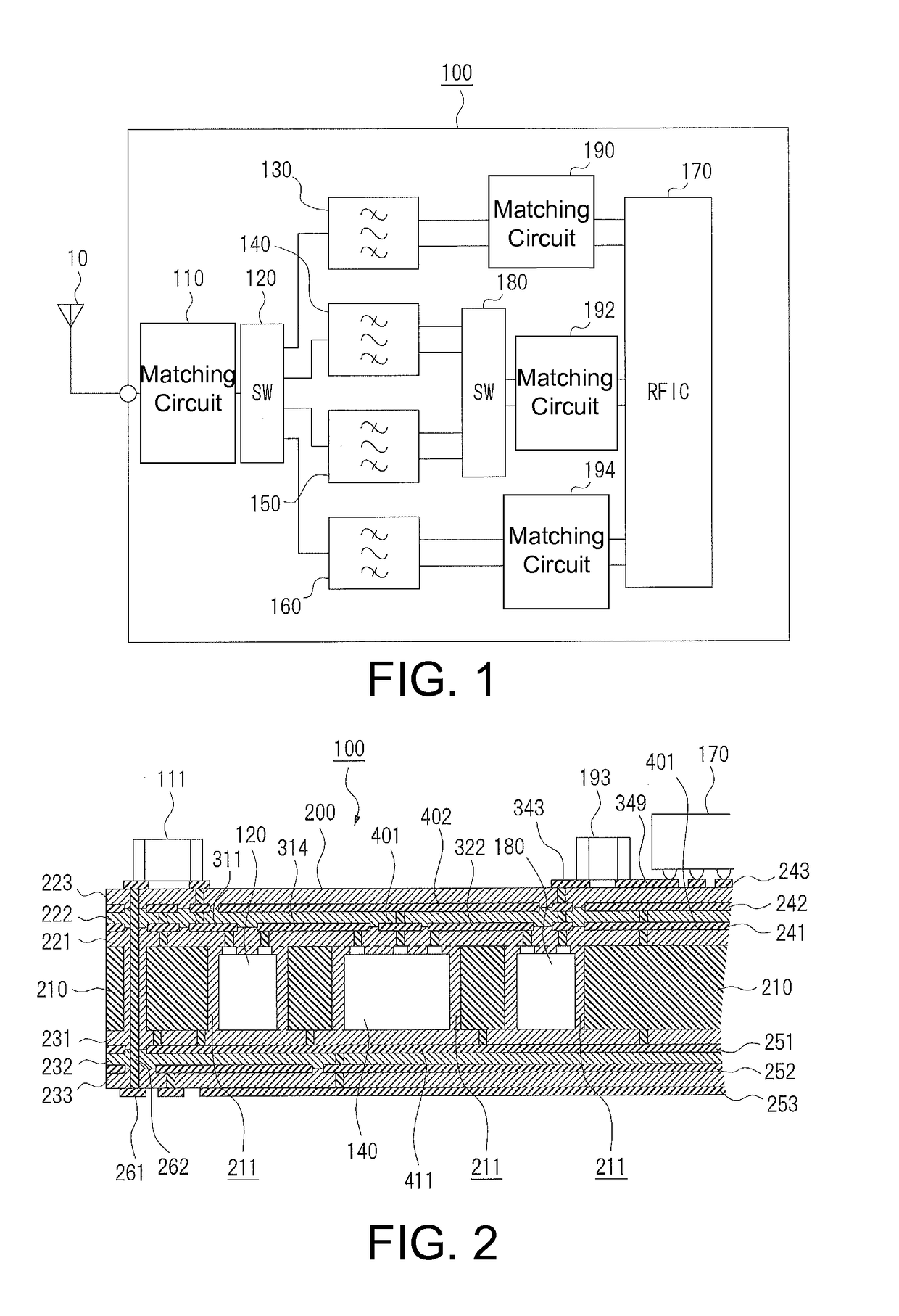
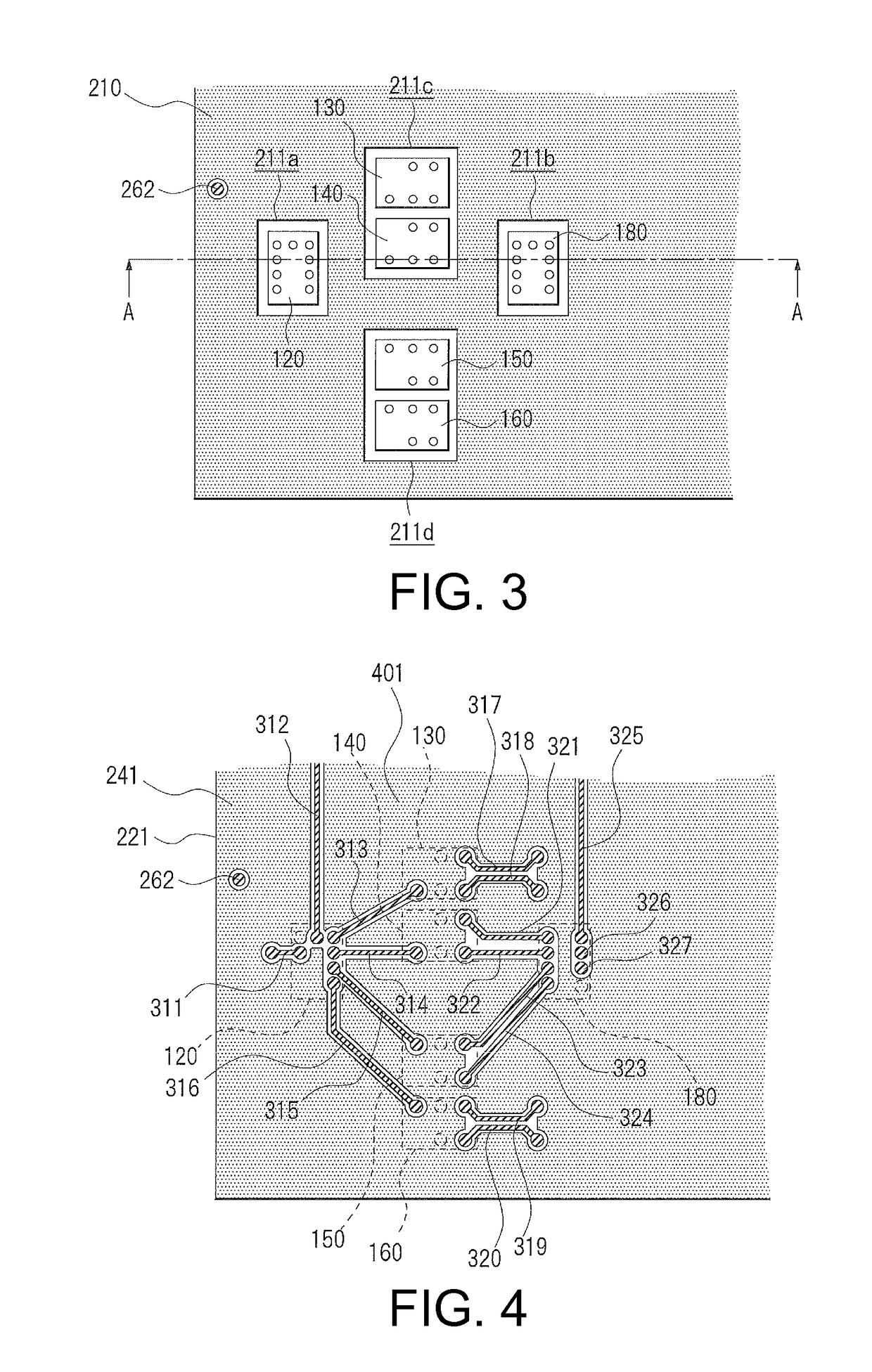
[0039]A high frequency circuit module according to Embodiment 1 of the present invention will be explained with reference to figures. FIG. 1 is a schematic circuit diagram of the high frequency circuit module. In the present embodiment, for simplicity of explanation, only main configurations relating to the gist of the present invention will be explained.

[0040]A high frequency circuit module 100 of the present embodiment is used for a mobile phone that handles four frequency bands. The high frequency circuit module 100 has a diversity configuration, and includes a pair of transmission / reception circuits for one antenna, and one reception circuit (a diversity reception circuit) for another antenna. In the present embodiment, for simplicity of explanation only the latter diversity reception circuit will be explained, and an explanation of the other circuits will be omitted. A transmission filter is also included in the former transmission / reception circuits.

[0041]As shown in FIG. 1, a...

embodiment 2

[0061]A high frequency circuit module according to Embodiment 2 of the present invention will be explained with reference to figure. The high frequency circuit module of the present embodiment differs from Embodiment 1 in regards to the layered structure of the multilayer circuit substrate. Other features are the same as in Embodiment 1, and thus only the differences will be explained. Configurations that are similar to Embodiment 1 are given the same reference characters.

[0062]FIG. 7 is a cross-sectional view of the high frequency circuit module according to Embodiment 2. The multilayer circuit substrate 200 of Embodiment 1 had the core layer 210 at the center with three layers each of insulating layers and conductive layers on both surfaces of the core layer 210. A multilayer circuit substrate 200a of the present embodiment differs from Embodiment 1 in that a core layer 210 at the center has four layers each of insulating layers and conductive layers on both surfaces of the core l...

embodiment 3

[0065]A high frequency circuit module according to Embodiment 3 of the present invention will be explained with reference to figures. FIG. 8 is a schematic circuit diagram of the high frequency circuit module. In the present embodiment, for ease of explanation, only main configurations relating to the gist of the present invention will be explained.

[0066]A high frequency circuit module 500 of the present embodiment is used for a mobile phone that handles four frequency bands. This high frequency circuit module 500 has a pair of transmission / reception circuits for one antenna.

[0067]As shown in FIG. 8, the high frequency circuit module 500 is provided with: a matching circuit 510 that matches with an antenna 50; a first high frequency switch 520 that switches the connection of the antenna 50 for each frequency band; first to fourth duplexers 530, 540, 550, and 560 that electrically isolate transmission signals and reception signals in order to perform transmission and reception with t...


PUM


Abstract

A high frequency circuit module is provided with: a multilayer circuit substrate; a first high frequency switch that switches connection of an antenna; a transmission filter; and reception filters. Either the transmission filter or the reception filters, or both, and the first high frequency switch are embedded in the multilayer circuit substrate, and ground conductors are formed in a conductive layer facing embedded electronic components.

Description

[0001]This application claims the benefit of Japanese Application No. 2013-082835, filed in Japan on Apr. 11, 2013, which is hereby incorporated by reference in its entirety.BACKGROUND OF THE INVENTION[0002]Field of the Invention[0003]The present invention relates to a high frequency circuit module in which high frequency circuits are mounted on a multilayer circuit substrate, and particularly relates to a mounting structure of a high frequency switch and filters.[0004]Description of Related Art[0005]Conventionally, switching circuits utilizing PIN diodes have been employed in circuit modules including high frequency switches used for mobile phones. However, with a recent trend of handling multiple bands and higher communication frequency bands, high frequency switches utilizing FET switches have been more widely used. Known examples of circuit modules with these types of high frequency switches include the circuit modules disclosed in Patent Documents 1 to 3. A high frequency switc...

Claims


Application Information

Patent Timeline
Patent Type & Authority Patents(United States)
IPC IPC(8): H04B1/44H01L23/00H01L23/538H04B1/04H04B1/18H04B1/48
CPCH04B1/48H01L23/5389H01L24/19H04B1/0458H04B1/18H01L2924/19105H01L23/5386H01L2224/04105H01L2224/16225H01L2224/24137H01L2224/73267H01L23/5384
Inventor SAJI, TETSUONAKAMURA, HIROSHI
Owner TAIYO YUDEN KK
Why Eureka
Try Eureka