Structured illumination device and structured illumination microscope device

a microscope device and structure technology, applied in the direction of instruments, optical elements, fluorescence/phosphorescence, etc., can solve the problem of not being able to achieve the desired super-resolution effect at all

Inactive Publication Date: 2018-02-20
NIKON CORP
View PDF16 Cites 4 Cited by
  • Summary
  • Abstract
  • Description
  • Claims
  • Application Information

AI Technical Summary

Problems solved by technology

These light beams interfere in the area around the specimen, forming interference fringes which are used as the structured illumination light.
However, changing the wavelength of the light source in the structured illumination microscope changes the diffraction angle of the diffraction grating, thereby changing the distance of the illumination light spots from the radius of the pupil of the objective lens, and in some cases, making it no longer possible to achieve the desired super-resolution effect at all.

Method used


Image

  • Structured illumination device and structured illumination microscope device
  • Structured illumination device and structured illumination microscope device
  • Structured illumination device and structured illumination microscope device

Examples


embodiment 1

[0048]Next, a structured illumination microscope device according to Embodiment 1 of the present invention will be described.

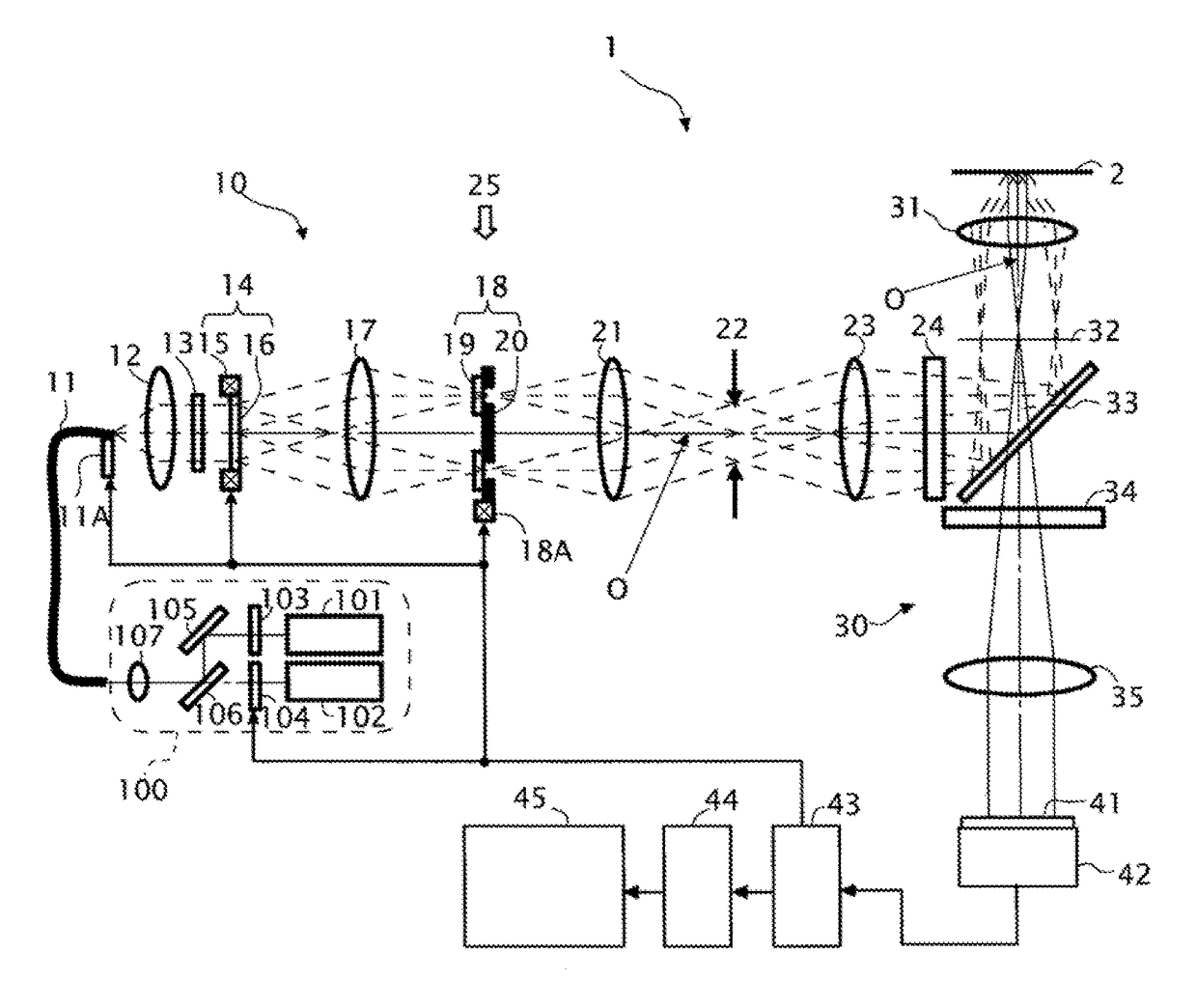
[0049]FIG. 1 illustrates the configuration of a structured illumination microscope device 1. In the following description, the structured illumination microscope device 1 is used as a total internal reflection fluorescence microscope (TIRFM) as an example—in other words, the structured illumination microscope device 1 is used in a TIRFM-SIM mode. TIRFM-SIM mode refers to a mode in which an extremely thin layer of the surface of a sample (specimen) 2 that exhibits fluorescence is observed.

[0050]First, the configuration of the structured illumination microscope device 1 will be described.

[0051]As illustrated in FIG. 1, the structured illumination microscope device 1 includes a laser unit 100, an optical fiber 11, an illumination optical system 10, an imaging optical system 30, an image sensor 42, a control device 43, an image storage / processing device 44, and an...

embodiment 2

[0169]Next, a structured illumination microscope device according to Embodiment 2 of the present invention will be described.

[0170]The structured illumination microscope device according to the present embodiment is a modification example of the structured illumination microscope device according to Embodiment 1, and therefore only the differences between the present embodiment and Embodiment 1 will be described here.

[0171]In Embodiment 1, the structured illumination microscope device 1 is used in a total internal reflection fluorescence structured illumination microscope mode (TIRF-SIM mode). In the present embodiment, however, the structured illumination microscope device 1 can be switched between the total internal reflection fluorescence structured illumination microscope mode (TIRF-SIM mode) and a total internal reflection fluorescence microscope mode that does not use structured illumination (TIRF mode).

[0172]In TIRF-SIM mode, although the sample 2 can be observed at a high re...

embodiment 3

[0223]Next, a structured illumination microscope device according to Embodiment 3 of the present invention will be described.

[0224]The structured illumination microscope device according to the present embodiment is a modification example of the structured illumination microscope device according to Embodiment 1, and therefore the following description focuses on the differences between the present embodiment and Embodiment 1.

[0225]In Embodiment 1, the light-collecting optical system is given a prescribed chromatic aberration of magnification in order to reduce changes in the distance from the optical axis O to the focused light spots on the pupil plane of the objective lens (due to changes in the diffraction angle) when switching between wavelengths. However, in the present embodiment, changes in the distance from the optical axis O to the focused light spots on the pupil conjugate plane of the objective lens (due to changes in the diffraction angle) are reduced when switching betw...


PUM

PropertyMeasurementUnit
wavelengthsaaaaaaaaaa
reference wavelength λ0aaaaaaaaaa
wavelengthaaaaaaaaaa

Abstract

A structured illumination device includes: a diffraction unit that diffracts light beams of a plurality of wavelengths that are emitted simultaneously or sequentially by a light source into a plurality of diffracted beams; and an optical system that forms interference fringes on a surface of a sample using the plurality of diffracted beams diffracted by the diffraction unit, the optical system including a first optical system and a second optical system that focuses the plurality of diffracted beams at positions on or near a pupil plane of the first optical system, and a magnification characteristic dY(λ) of the second optical system satisfying the condition of (fo·nw−afλ / P)≦dY(λ)≦(fo·NA−afλ / P), where a=1 (for M=1, 2) or a=2 (for M=3).

Description

CROSS REFERENCE TO THE RELATED APPLICATIONS[0001]This application is a continuation application of International Application PCT / JP2014 / 002855, filed May 29, 2014, designating the U.S., and claims the benefit of priority from Japanese Patent Application No. 2013-148730, filed on Jul. 17, 2013, the entire contents of which are incorporated herein by reference.BACKGROUND[0002]1. Field[0003]The present invention relates to a structured illumination device and a structured illumination microscope device.[0004]2. Description of the Related Art[0005]In the fields of observation and measurement of samples (specimens), structured illumination microscopes (SIM) have been proposed as one way of achieving resolutions that exceed the performance of objective lenses (see Patent Document 1: US Reissued Patent Application Publication No. 38307, for example). In a structured illumination microscope, the sample is illuminated with spatially modulated illumination light (structured illumination light...

Claims


Application Information

Patent Timeline
Patent Type & Authority Patents(United States)
IPC IPC(8): G01N21/64G02B21/06G02B21/00G02B21/36G02B27/58G02B21/16
CPCG02B21/06G01N21/64G01N21/6428G02B21/0032G02B21/0076G02B21/367G02B27/58G02B21/16G01N2201/0638G01N2021/6439G01N2201/063G01N21/6458
Inventor NAKAYAMA, HIROAKIOUCHI, YUMIKO
Owner NIKON CORP
Why Eureka
Try Eureka