Modular surface mount component for an electrical device or LED's

a technology of leds and modules, applied in the direction of sustainable manufacturing/processing, identification means, instruments, etc., can solve the problems of large cost of interface devices such as displays, increasing the cost of displaying information, so as to achieve a significant reduction in manufacturing costs

Inactive Publication Date: 2000-03-14
OSRAM OPTO SEMICONDUCTORS GMBH & CO OHG +1
View PDF14 Cites 77 Cited by
  • Summary
  • Abstract
  • Description
  • Claims
  • Application Information

AI Technical Summary

Benefits of technology

An object of the present invention is to provide a novel and improved method of manufacturing modular components in which the manufacturing costs are considerably lower than those known from the prior art and in which at the same time the packaging features are at least the equal of those known from the prior art.

Problems solved by technology

However, with the advances in integrated circuitry technology progressively providing increased processing power in smaller space at reduced costs, the cost of interface devices, such as displays, becomes a larger portion of the total cost and thus more significant.
Also when the cost of displaying information is low, the additional cost of displaying more information when desirable is not a deterent leading to greater design freedom.

Method used


Image

  • Modular surface mount component for an electrical device or LED's
  • Modular surface mount component for an electrical device or LED's
  • Modular surface mount component for an electrical device or LED's

Examples


Embodiment Construction

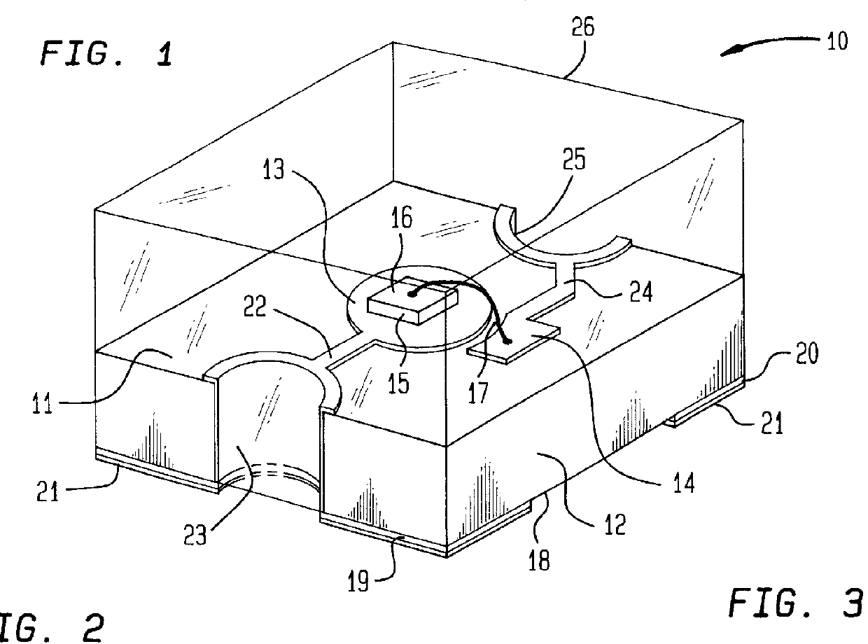
FIG. 1 demonstrates the construction of a typical modular component 10 that may be manufactured according to the present invention. Deposited onto the upper side 11 of a flat substrate 12 of an electrically insulating material, for instance synthetic plastic material or the like, is a conductive pattern of highly conductive material such as copper. The conductive pattern deposited onto the upper side 11 defines a land area 13 and a connection pad 14. A light emitting diode 15 is mounted on the land area 13 so that its terminal on the underneath or back side is electrically and mechanically coupled to the land area 13. The upper side of the light emitting diode 15 is provided with a terminal 16 which is electrically conductive and connected with the connection pad 14 via a bonding wire 17.

Deposited onto the rear of back side 18 of the flat substrate 12 is a second conductive pattern of highly conductive material such as copper. This second conductive pattern defines a first terminal ...


PUM


Abstract

Processing techniques for various surface mount modular components provide various structures for single device components (10) and multiple device components (FIGS. 6 and 7) suitable as character displays. The technique beings with a slab of substrate material 12 patterned on both sides. Plated through holes (33, 43) connecting back side terminals (19, 20) to front side connective strips (22, 24) are formed. Devices (15, 16) are mounted to land areas (13, 34) and wire bonded to connecting pads (14). The front side is coated with epoxy to encapsulate the devices in a layer having an outer surface formed into optional lenses (262, 263). The slab is then separated to provide the modular components.

Description

BACKGROUND OF THE INVENTIONThis invention relates to electro-optical displays and other modular compact components. In particular, the invention relates to a method of manufacturing such components capable of being fully automated for producing low cost modular components also highly suitable for automated assembly in installations.Display devices are used extensively particularly in digital circuitry to provide information for the interface for the user. However, with the advances in integrated circuitry technology progressively providing increased processing power in smaller space at reduced costs, the cost of interface devices, such as displays, becomes a larger portion of the total cost and thus more significant. Also when the cost of displaying information is low, the additional cost of displaying more information when desirable is not a deterent leading to greater design freedom. In view of these economic or cost saving benefits, it is extremely desirable to have a fully autom...

Claims


Application Information

Patent Timeline
Patent Type & Authority Patents(United States)
IPC IPC(8): H01L33/00G09F9/33H01L25/075H01L33/48H01L33/54H05K3/34
CPCG09F9/33H01L33/54H05K3/3442H01L33/486H05K2201/09181H05K2201/10106H05K2201/10128H01L2224/48091H01L2224/48227H01L2924/00014Y02P70/50
Inventor LUMBARD, MARVINWIESE, LYNN K.
Owner OSRAM OPTO SEMICONDUCTORS GMBH & CO OHG
Why Eureka
Try Eureka