Method of multi-level storage in DRAM and apparatus thereof

Inactive Publication Date: 2001-02-27
MOSAID TECH
View PDF7 Cites 7 Cited by
  • Summary
  • Abstract
  • Description
  • Claims
  • Application Information

AI Technical Summary

Benefits of technology

In the present invention a method and circuit has been designed which substantially solves .Iadd.some of .Iaddend.the above-identified problems. Only two sense amplifiers are required.[., which generate the sensing voltages at the time of sensing.]. . In the present invention each bitline is split exactly in half, rather than into thirds, by

Problems solved by technology

A problem with such cells, is that noise margins are reduced to one-third that of a one bit per cell DRAM, which is too low to withstand the occasional .alpha.-particle bit.
A second problem with multi-bit storage cells relates to the method of sensing.
These levels are not self-compensated for offsets developed in the sensing operation, and this method suffers from poor signal margin.
Leakage characteristics of the

Method used


Image

  • Method of multi-level storage in DRAM and apparatus thereof
  • Method of multi-level storage in DRAM and apparatus thereof
  • Method of multi-level storage in DRAM and apparatus thereof

Examples


Embodiment Construction

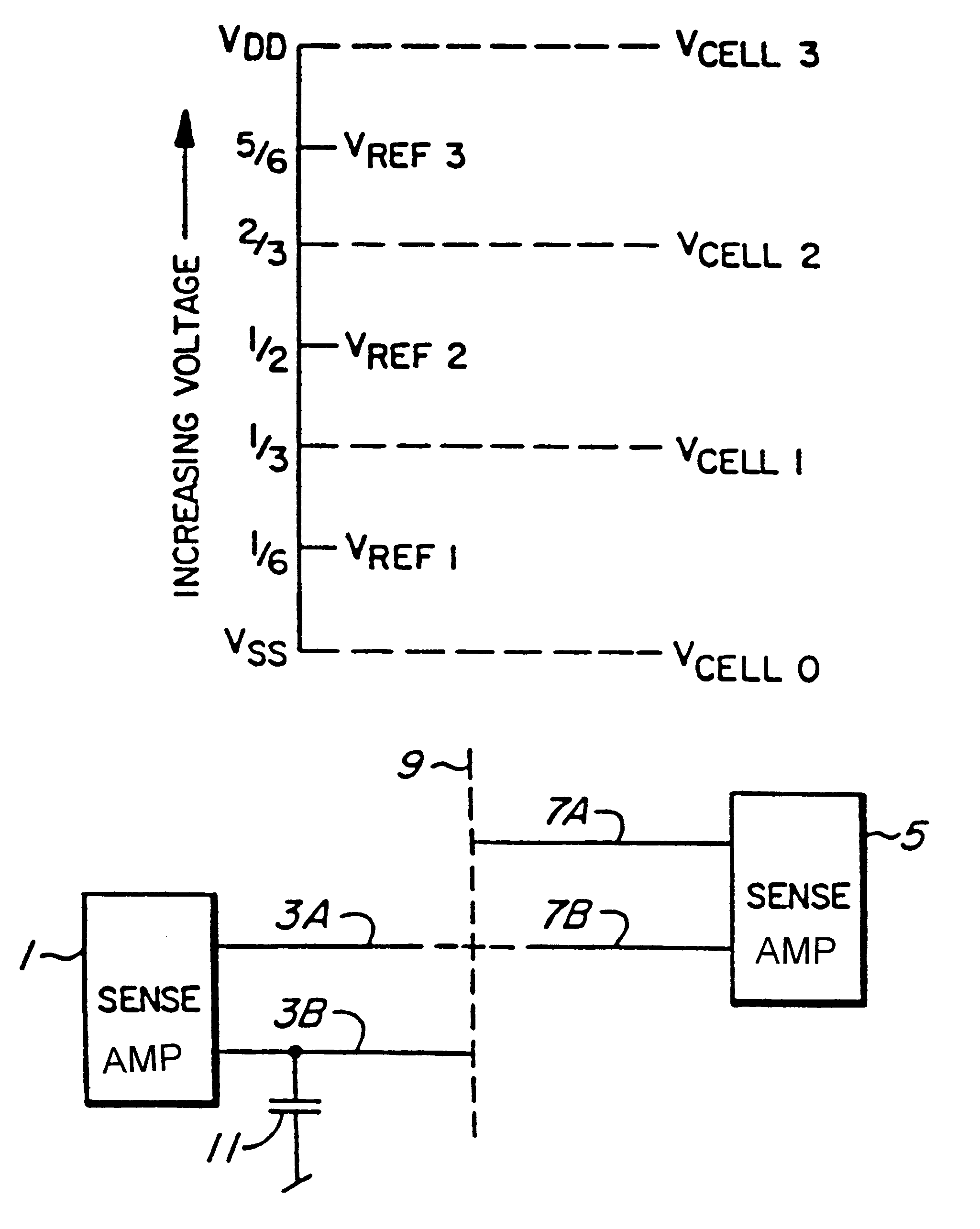
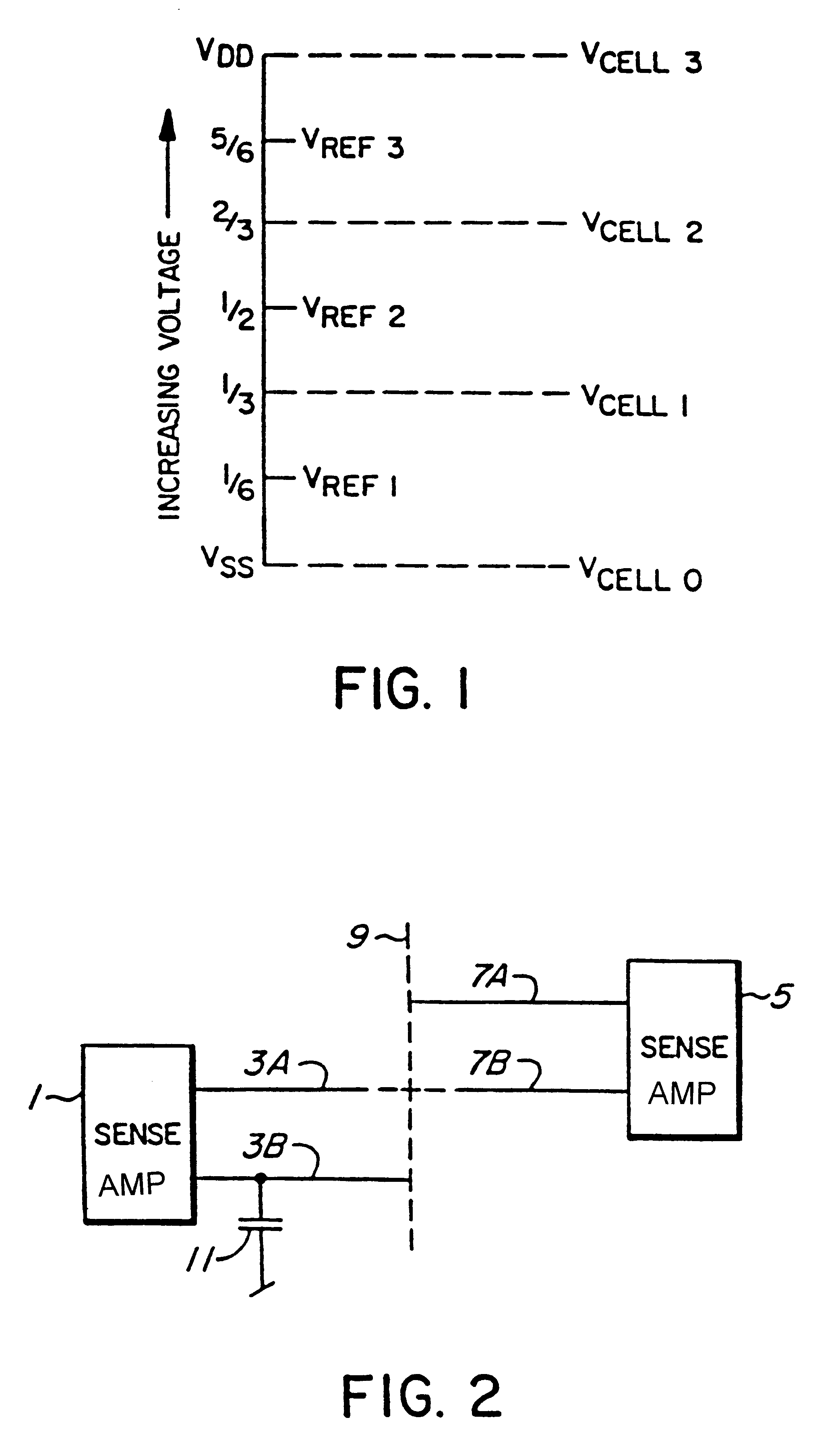
For a DRAM cell to store two bits using a single cell capacitor, the cell capacitor should store one of four voltage values V.sub.cell0, V.sub.cell1, V.sub.cell2 or V.sub.cell3, wherein V.sub.cell0 represents the lowest and V.sub.cell3 represents the highest cell voltage. To differentiate between the voltages, mid-point voltages V.sub.ref1 V.sub.ref2 and V.sub.ref3 are defined, as shown in FIG. 1. It may be seen that if the lowest actual cell voltage V.sub.cell0 is V.sub.SS or zero, V.sub.ref1 is one-sixth the highest voltage V.sub.DD, V.sub.cell1 is one-third V.sub.DD, V.sub.ref2 is one-half V.sub.DD, V.sub.cell2 is two-thirds V.sub.DD, V.sub.ref3 is five-sixths V.sub.DD and V.sub.cell3 equals V.sub.DD. Thus it may be sen that V.sub.ref1 is midway between V.sub.cell0 and V.sub.cell1, V.sub.ref2 is midway between V.sub.cell0 and V.sub.cell3 and V.sub.ref3 is midway between V.sub.cell2 and V.sub.cell3.

FIG. 2 will be used to illustrate the basic concept of the invention. A sense ampli...


PUM


Abstract

A method of processing data having one of four voltage levels stored in a DRAM cell is comprised of sensing whether or not the data voltage is above or below a voltage level midway between a highest and a lowest of the four levels, setting the voltage on a reference line higher than the lowest and lower than the next highest of the four levels in the event the data voltage is below the midway voltage level, and setting the voltage on the reference line higher than the second highest and lower than the highest of the four levels in the event the data voltage is above the midway point, and sensing whether the data voltage is higher or lower than the reference line, whereby which of the four levels the data occupies is read.

Description

FIELD OF THE INVENTIONThis invention relates to dynamic random access memory (DRAM) memories, and in particular to a method of storing a variable level signal in each cell of a DRAM for representing more than one bit in each cell.BACKGROUND OF THE INVENTIONTo store for example two bits in a DRAM cell, it must be able to store four different voltage levels. A problem with such cells, is that noise margins are reduced to one-third that of a one bit per cell DRAM, which is too low to withstand the occasional .alpha.-particle bit.A second problem with multi-bit storage cells relates to the method of sensing. No simple method of sensing has previously been designed, although attempts have been made to solve this problem, e.g. as described in the publication by M. Aoki, et al, "A 16-Levels / Cell Dynamic Memory", ISSCC Dig. TECH. Papers 1985, pp. 246-247, and in T. Furuyama et al, "An Experimental Two-Bit / Cell Storage DRAM for Macrocell or Memory-On-Application", IEEE Journal of Solid State...

Claims


Application Information

Patent Timeline
IPC IPC(8): G11C11/56
CPCG11C11/565G11C7/06G11C2211/5634
Inventor GILLINGHAM, PETER B.
Owner MOSAID TECH
Why Eureka
Try Eureka