Liquid crystal display device and manufacturing method thereof

Inactive Publication Date: 2002-12-31
SEIKO EPSON CORP
View PDF23 Cites 11 Cited by
  • Summary
  • Abstract
  • Description
  • Claims
  • Application Information

AI Technical Summary

Benefits of technology

Therefore, it is the object of the present invention to solve the above-mentioned problems and provide a new structure for

Problems solved by technology

Such conventional devices have numerous drawbacks problems and has a disadvantage for example in the above-mentioned conventional liquid crystal display device, it is necessary to fill and coat the gap between top substrate 1 and bottom substrate 2 with resin molding material 8 in order to secure the area where electrode pads 3a and 4a and insertion pins 7 with legs are conductively connected, and to prevent electrolytic corrosion of electrode pads 4a, in the electrode lead-out area where bottom substrate 2 extends outward beyo

Method used


Image

  • Liquid crystal display device and manufacturing method thereof
  • Liquid crystal display device and manufacturing method thereof
  • Liquid crystal display device and manufacturing method thereof

Examples


first embodiment

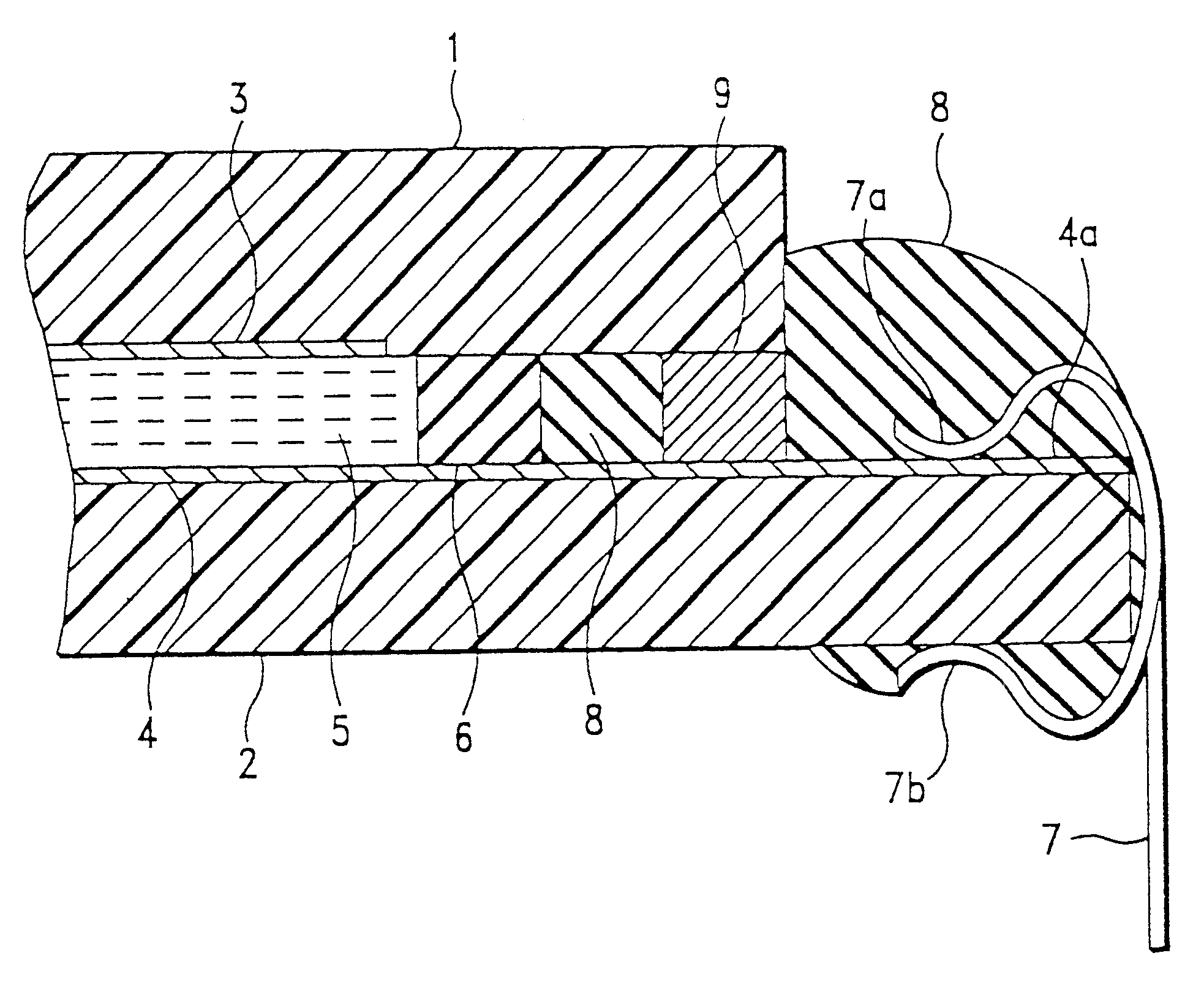
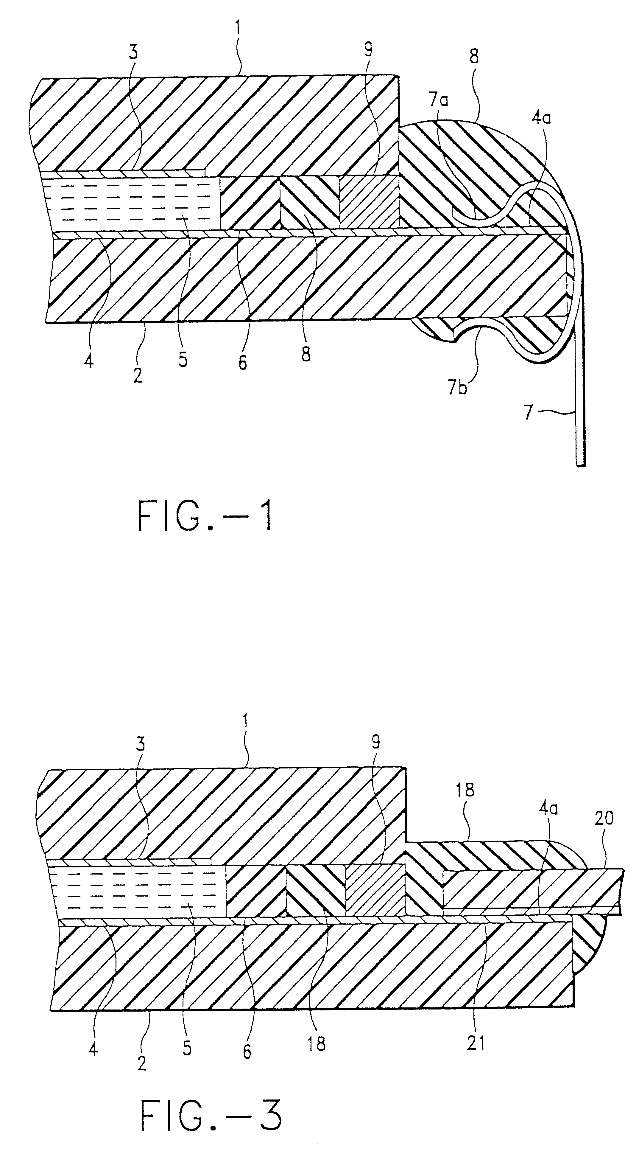
FIG. 1 shows an enlarged partial cross-sectional view of the first embodiment of the liquid crystal display device related to the invention. In this embodiment, the liquid crystal display device is provided with top substrate 1 formed in the same way as the conventional example described above, bottom substrate 2, transparent electrodes 3 and 4. Liquid crystal layer 5, seal material 6, and electrode pads 4a. Insertion pins 7 with legs are installed on electrode pads 4a of bottom substrate 2 and are then fastened with molding material 8. Depending on the liquid crystal display method, a polarizing plate may be positioned on the outside of the top and bottom substrates.

In this embodiment, support columns 9 formed using a conductive ink containing carbon particles are formed between the edges of top substrate 1 and bottom substrate 2. As will be explained below, these support columns 9 are formed simultaneously with the assembly of the top and bottom substrates before mold material 8 i...

second embodiment

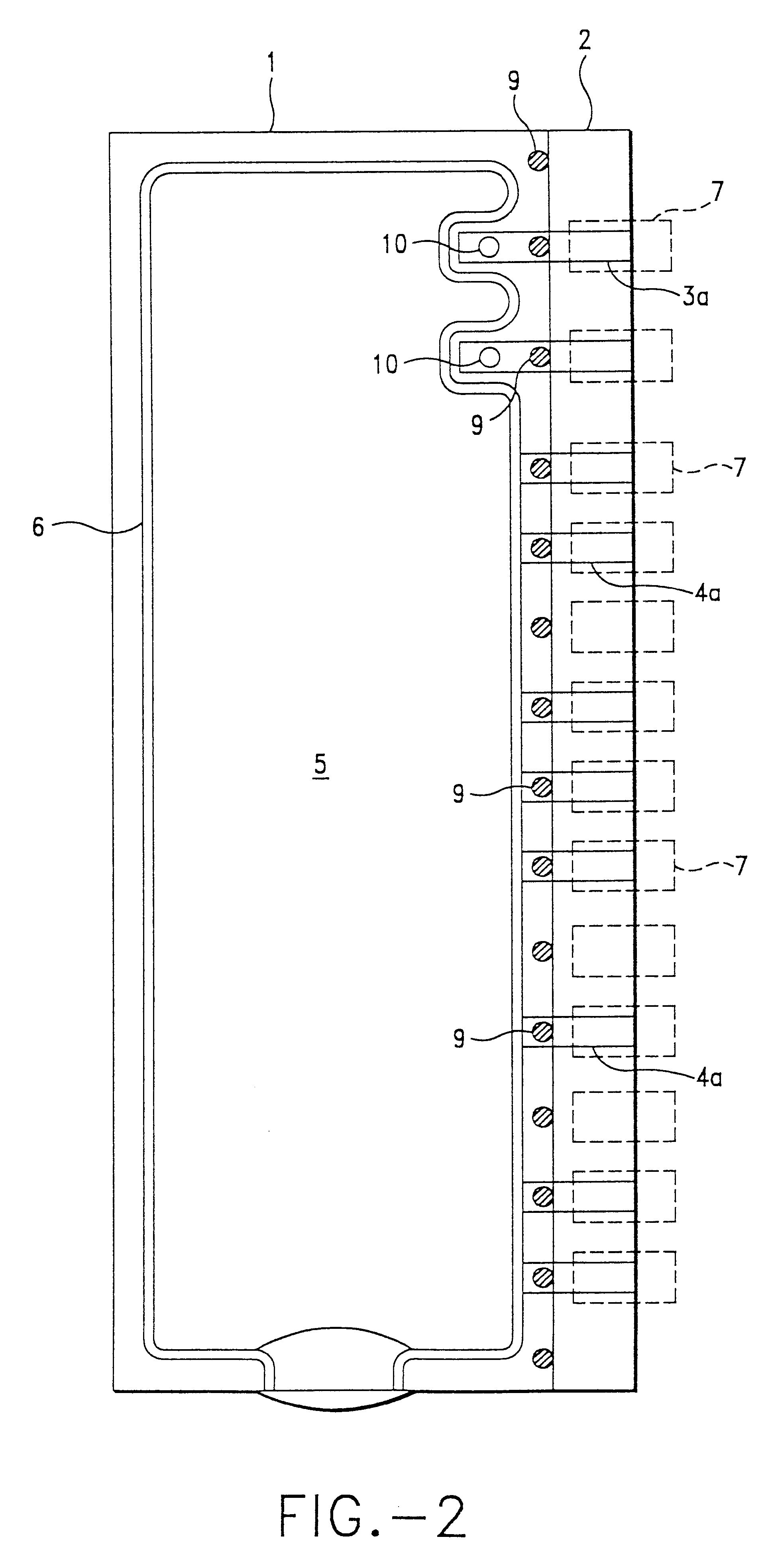
FIG. 3 shows the second embodiment of the liquid crystal display device related to the invention. In the second embodiment, top substrate 1, bottom substrate 2, transparent electrodes 3 and 4, electrode pads 4a, liquid crystal layer 5, seal material 6, and support columns 9 are identical to those in the above embodiment, and thus their explanations are omitted.

In this embodiment, heat seal 20 is adhered to the top of multiple and parallel electrode pads 3a (connected to transparent electrode 3; FIG. 6) and 4a. In heat seal 20, wiring pads 21 are formed on the bottom of a thin flexible resin sheet at the same pitch as that of electrode pads 3a and 4a, and an anisotropic conductive layer (not shown in the figure) is adhered to the surface of wiring pads 21. This anisotropic conductive layer is produced by dispersing conductive particles in a thermohardening resin, for example, and adhesion with appropriate heating and pressurization can produce conductivity in the adhesion direction o...


PUM


Abstract

In a liquid crystal display device, support columns are formed on the outside of a seal area in an edge area of opposing substrates, thus reducing substrate deformation and preventing the occurrence of air bubbles inside the liquid crystal layer, undesirable coloring of the display area, and color irregularity. Support columns 9 formed using a conductive ink are provided on the outside of seal material 6 used for sealing liquid crystal layer 5 contained between top substrate 1 and bottom substrate 2. The support columns 9 prevent the warping of substrates 1 and 2 caused by the shrinkage of mold material 8 during hardening, reducing the changes in the liquid crystal layer thickness. Support columns 9 are print-formed simultaneously with the conductive connection area of the liquid crystal panel, and are hardened simultaneously with the seal material.

Description

BACKGROUND OF THE INVENTION1. Field of the InventionThe invention relates to a liquid crystal display device, and more particularly to technologies for enhancing the structure of the peripheral area of the substrate of a liquid crystal display.2. Description of the Related ArtIn conventional liquid crystal display devices, the sealing of a liquid crystal layer between two substrates, and the application of voltage between the electrodes formed in pairs on the back side of the liquid crystal layer change the orientation of the liquid crystals inside the layer, making it possible to display various images. FIG. 7 depicts an example of an enlarged cross-sectional view of the substrate edge area of a conventional liquid crystal display devices, and FIG. 8 is a perspective view from above showing the overall configuration.As shown therein, both the top and bottom substrates 1, 2 are constituted by clear glass plates, and transparent electrodes 3 and 4 are formed in specified patterns on ...

Claims


Application Information

Patent Timeline
IPC IPC(8): G02F1/1333G02F1/1339G02F1/13G02F1/1345G09F9/30
CPCG02F1/133351G02F1/1339
Inventor KANEZAWA, TATSUO
Owner SEIKO EPSON CORP
Why Eureka
Try Eureka