
Two-dimensional beam deflector

a beam deflector and beam deflector technology, applied in the field of two-dimensional beam deflectors, can solve the problems of interfering one with the other, spectrophotometers having difficulty measuring structures with very small reflectance, and spectrophotometers also having difficulty measuring films with unknown or unrepeatable dispersions of optical constants

Inactive Publication Date: 2003-06-24
NOVA MEASURING INSTR LTD
View PDF24 Cites 23 Cited by
  • Summary
  • Abstract
  • Description
  • Claims
  • Application Information

AI Technical Summary

Problems solved by technology

The spectrophotometer utilizes the fact that light beams reflected off thin film boundaries, will interfere one with another.
The spectrophotometers have difficulty measuring structures with very small reflectance, such as thin films of glass substrates, because the relatively low brightness of traditional white light sources does not provide a sufficient signal-to-noise ration (SNR).
Spectrophotometers also have difficulty measuring films with unknown or unrepeatable dispersions of optical constants, such as amorphous silicon.
Because ellipsometers measure two polarization parameters (amplitude and phase), both of which are independent of the light intensity, they are quite accurate and can also measure ultra thin films of the size of 0-100 .ANG.. However, since ellipsometers require oblique illumination as well as a highly collimated light beam, their use for high spatial resolution measurements in dense patterned structures is rather difficult.
This limits the speed with which a thickness mapping can occur, especially during inspection of large size substrates such as 8.DELTA.
They cannot be utilized for in-process control, since wafer handling and other mechanical movements are not allowed within a vacuum chamber.

Method used


Image

  • Two-dimensional beam deflector
  • Two-dimensional beam deflector
  • Two-dimensional beam deflector

Examples


Embodiment Construction

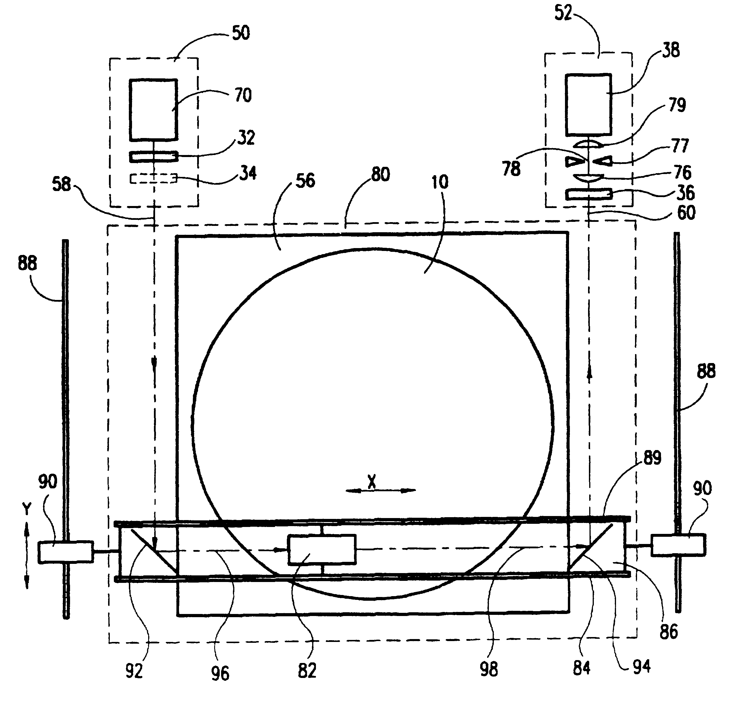
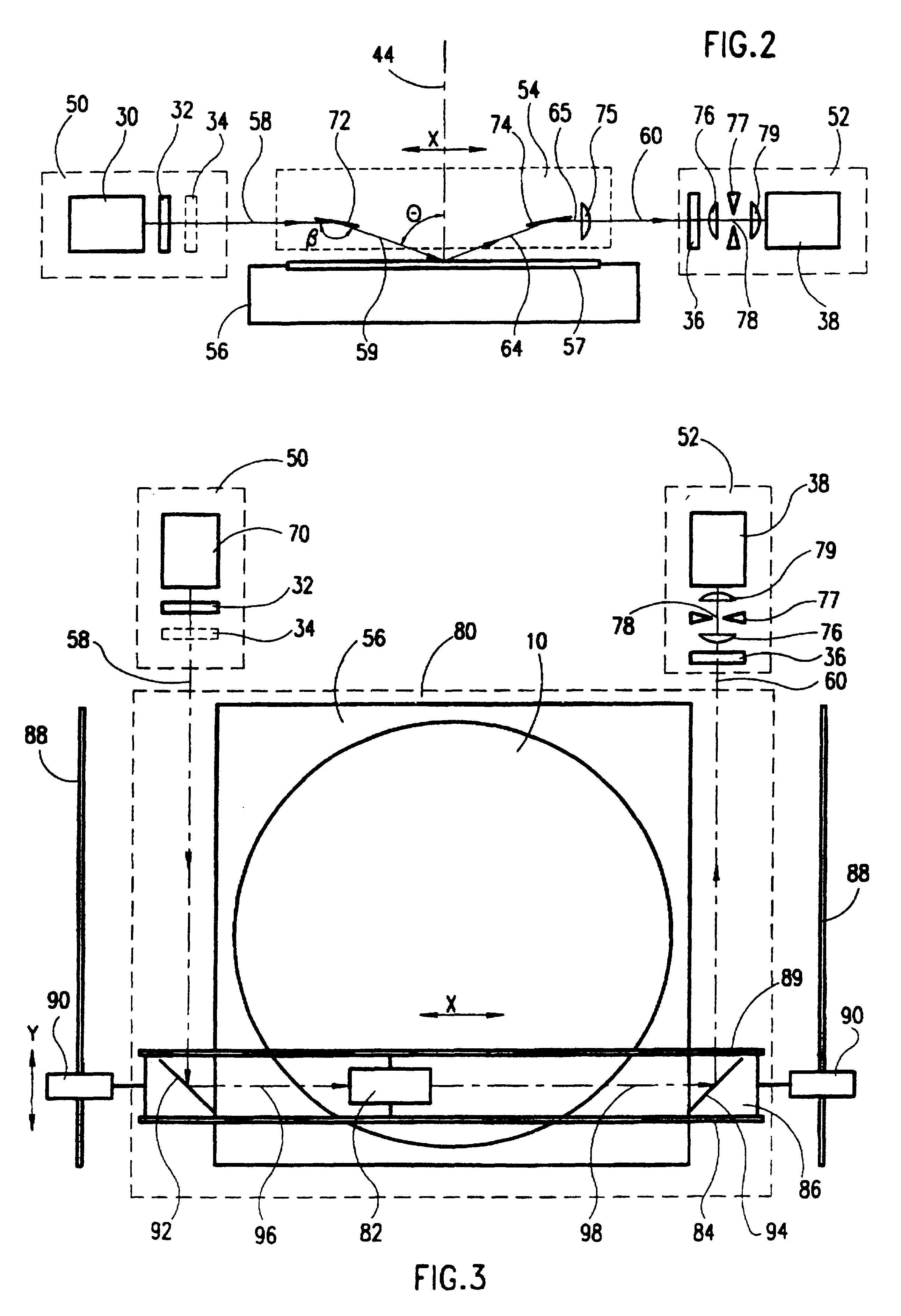
Reference is now made to FIGS. 2 and 3 which schematically illustrate an optical measuring device having one and two-dimensional scanning devices, respectively, constructed and operative in accordance with preferred embodiments of the present invention. In FIG. 2 is a side view and FIG. 3 is a top view.

In FIGS. 2 and 3, the optical measuring device is an ellipsometer. This is by way of example only; the principles of the present invention can also be implemented in a spectrophotometer, as illustrated in FIG. 6, described in detail hereinbelow.

The ellipsometer of FIG. 2 typically comprises a stationary illuminator 50, a stationary detector 52, a translating beam deflector 54, and a stationary support 56, such as a stage, ring, etc., for holding a sample 57.

The illuminator 50 typically comprises of elements similar to those of the prior art. Therefore, similar elements have similar reference numerals.

Specifically, the illuminator 50 typically comprises transmitter 30 which includes a ...


PUM

PropertyMeasurementUnit
angle of incidenceaaaaaaaaaa
sizeaaaaaaaaaa
focal lengthaaaaaaaaaa

Abstract

A two dimensional beam deflector is disclosed which deflects beams from multiple optical assemblies. The input of beams of the multiple optical assemblies follow parallel optical paths until deflection to a wafer. An ellipsometer using a two-dimensional beam deflector is also disclosed.

Description

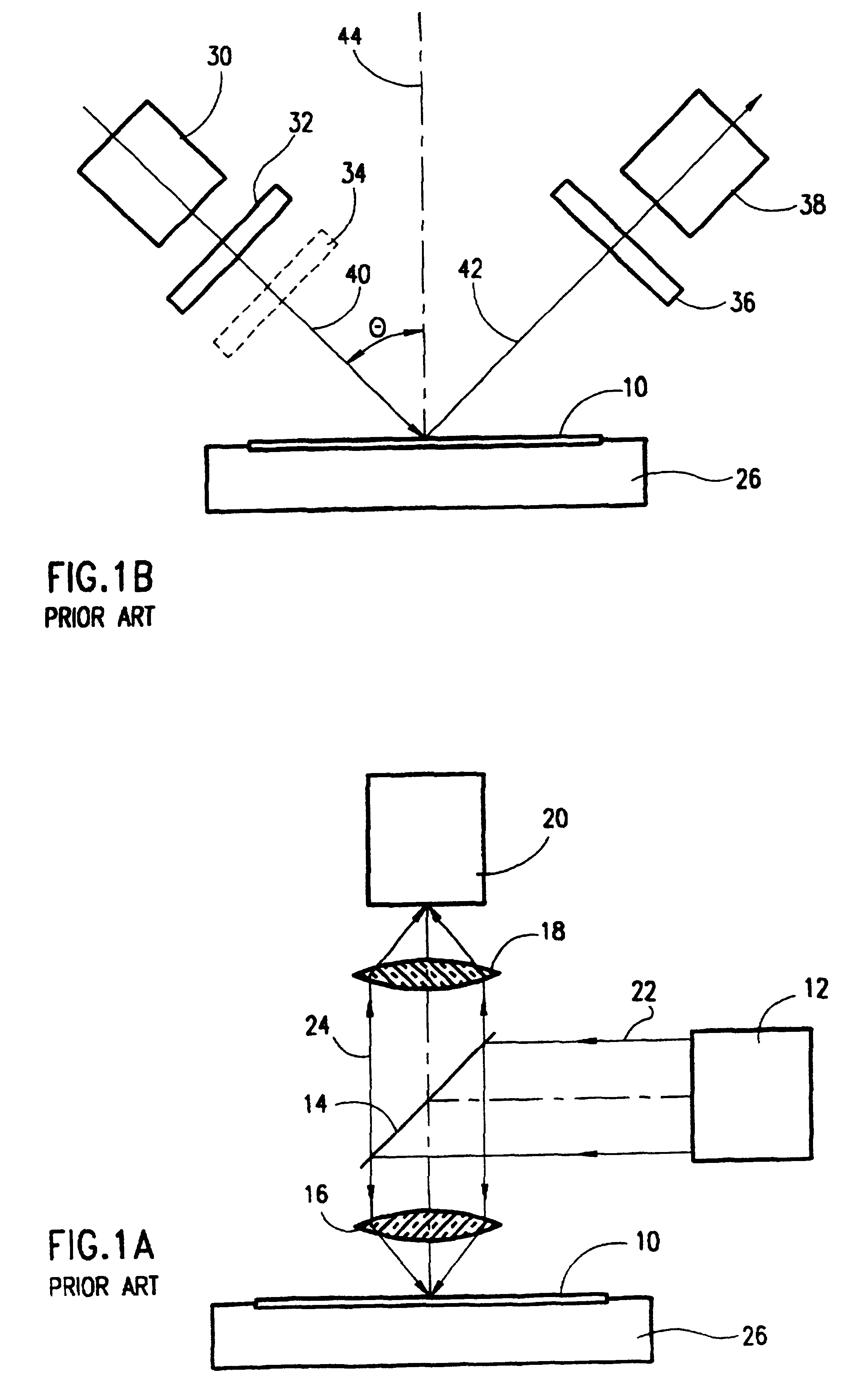
FIELD OF THE INVENTIONThe present invention relates to systems and methods for non-destructive quality control in general and to optical systems and methods for measuring the thickness and an index of refraction of thin films, in particular.BACKGROUND OF THE INVENTIONOptical measuring instruments are typically utilized in the microelectronic industry for non-contact, non destructive measurement of the thickness of thin films. Two main systems are utilized, spectrophotometers (or reflectometers) and ellipsometers. The following U.S. patents represent the prior art: For ellipsometers: U.S. Pat. Nos. 5,166,752, 5,061,072, 5,042,951, 4,957,368, 4,681,450, 4,653,924, 4,647,207 and 4,516,855. For spectrophotometers: U.S. Pat. Nos. 5,181.080, 5,159,412, 5,125,966, 4,999,014 and 4,585,348.The two prior art systems are illustrated in FIGS. 1A and 1B, respectively, to which reference is now made. The spectrophotometer utilizes the fact that light beams reflected off thin film boundaries, will...

Claims


Application Information

Patent Timeline
Patent Type & Authority Patents(United States)
IPC IPC(8): G01B11/06G03F7/20
CPCG01B11/065G02B26/0816G02B26/10G03F7/70358G03F7/704G03F7/70483G01B11/06G02B26/08
Inventor FINAROV, MOSHE
Owner NOVA MEASURING INSTR LTD
Learn More