Object observation apparatus and object observation

a technology of object observation and object beam, which is applied in the direction of material analysis, instruments, heat measurement, etc., can solve the problem that conventional apparatuses are difficult to realize high-precision observation of objects using electron beams, and achieve high precision

Inactive Publication Date: 2008-04-08
NIKON CORP
View PDF39 Cites 58 Cited by
  • Summary
  • Abstract
  • Description
  • Claims
  • Application Information

AI Technical Summary

Benefits of technology

[0008]It is, therefore, an object of the present invention to provide an observation apparatus and observation method capable of observing a clear image of an object to be observed at a high precision.

Problems solved by technology

However, the conventional apparatuses are difficult to realize high-precision observation of an object using an electron beam.

Method used


Image

  • Object observation apparatus and object observation
  • Object observation apparatus and object observation
  • Object observation apparatus and object observation

Examples


Embodiment Construction

[0024]An embodiment of the present invention will be described with reference to the accompanying drawings. The same reference numerals denote the same parts throughout the drawings, and a repetitive description thereof will be omitted.

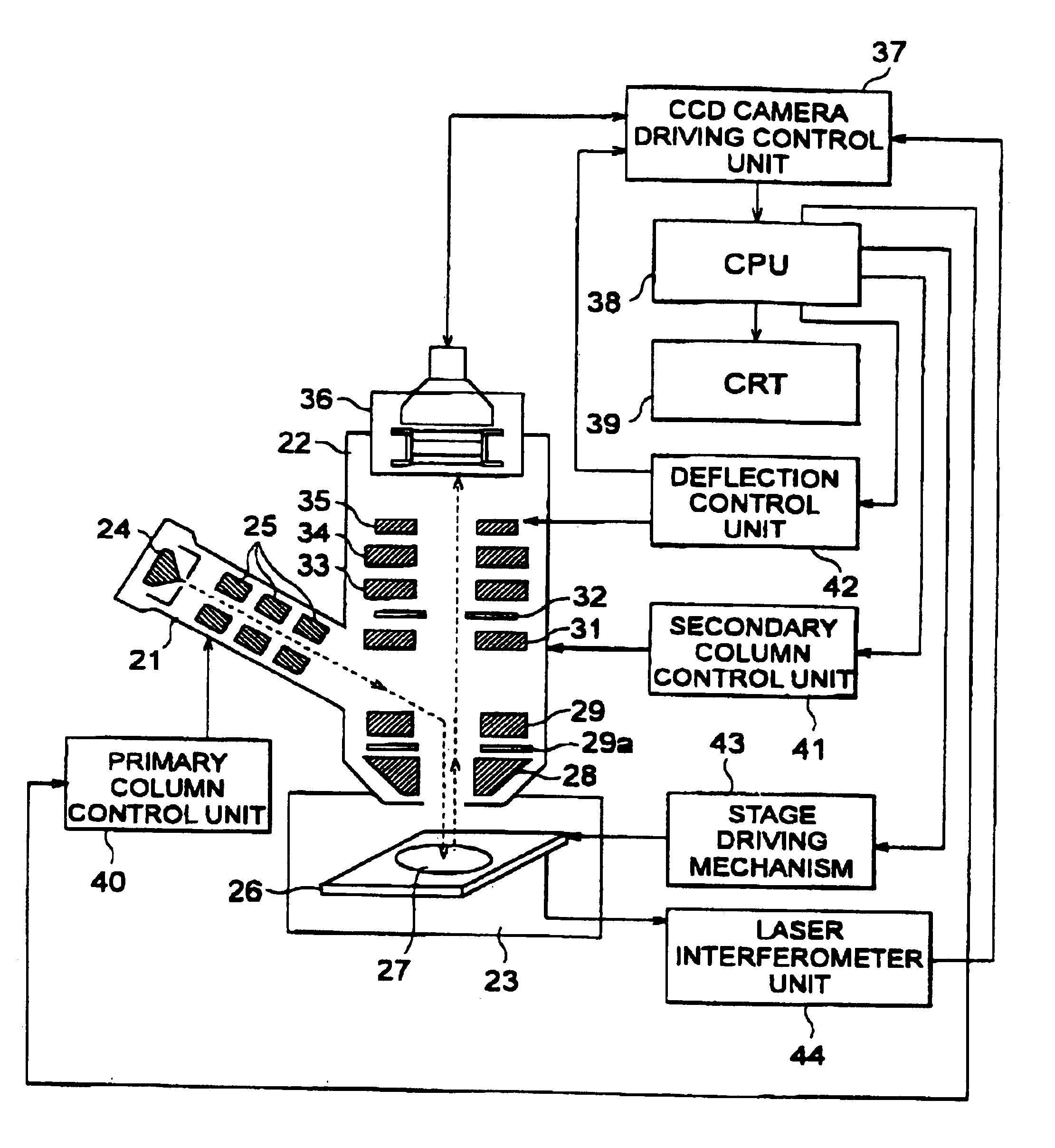
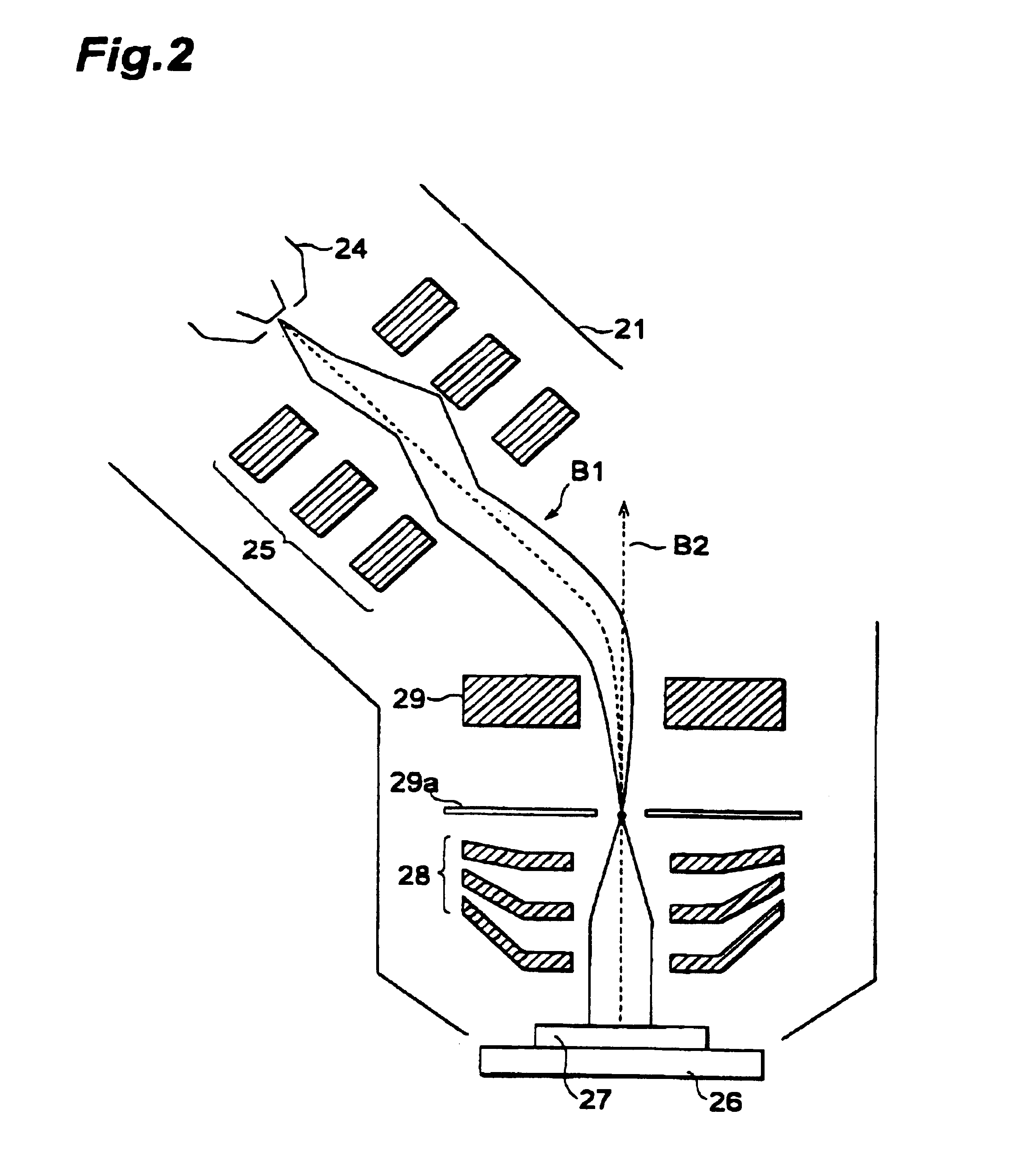
[0025]FIG. 1 is a view showing the whole arrangement of the embodiment. FIG. 2 is a view showing the structure of a primary column and the orbit of a primary beam. FIG. 3 shows views of the structure of an electrostatic lens in the primary column. FIG. 4 is a view showing the orbit of a secondary beam in a secondary column.

[0026]As shown in FIG. 1, an observation apparatus comprises a primary column 21, secondary column 22, and chamber 23.

[0027]The primary column 21 is diagonally connected to the side surface of the secondary column 22, and the chamber 23 is located below the secondary column 22.

[0028]The primary column 21 incorporates an electron gun 24. A primary optical system 25 is located on the optical path of an electron beam (primary beam) emi...


PUM

PropertyMeasurementUnit
pattern sizeaaaaaaaaaa
acceleration voltageaaaaaaaaaa

Abstract

This invention relates to an object observation apparatus and observation method. The object observation apparatus is characterized by including a drivable stage on which a sample is placed, an irradiation optical system which is arranged to face the sample on the stage, and emits an electron beam as a secondary beam, an electron detection device which is arranged to face the sample, causes to project, as a primary beam, at least one of a secondary electron, reflected electron, and back-scattering electron generated by the sample upon irradiation of the electron beam, and generates image information of the sample, a stage driving device which is adjacent to the stage to drive the stage, and a deflector arranged between the sample and the electron detection device to deflect the secondary beam, the electron detection device having a converter arranged on a detection surface to convert the secondary beam into light, an array image sensing unit which is adjacent to the converter, has pixels of a plurality of lines each including a plurality of pixels on the detection surface, sequentially transfers charges of pixels of each line generated upon reception of light of an optical image obtained via the converter to corresponding pixels of an adjacent line at a predetermined timing, adds, every transfer, charges generated upon reception of light after the transfer at the pixels which received the charges, and sequentially outputs charges added up to a line corresponding to an end, and a control unit connected to the array image sensing unit to output a transfer signal for sequentially transferring charges of pixels of each line to an adjacent line, and the control unit having a stage scanning mode in which the array image sensing unit is controlled in accordance with a variation in projection position of the secondary beam projected on the electron detection device that is generated by movement of the stage device, and a deflector operation mode in which the array image sensing unit is controlled in accordance with a variation in projection position of the secondary beam projected on the detection device by the deflector.

Description

RELATED APPLICATIONS[0001]This is a Continuation-in-part application of International Patent Application Serial No. PCT / JP98 / 03667 filed on Aug. 19, 1998, now pending.BACKGROUND OF THE INVENTION[0002]1. Field of the Invention[0003]The present invention relates to an object observation apparatus and, more particularly, to an apparatus and method of observing the integrated circuit pattern of a semiconductor wafer or the like using, e.g., an electron beam.[0004]2. Related Background Art[0005]With higher integration degrees of recent LSIs, the defect detection sensitivity required for samples such as a wafer and mask is increasing. For example, to detect defective portions on a wafer pattern 0.25 μm in DRAM pattern size, a detection sensitivity of 0.1 μm is required. In addition, demands have arisen for inspection apparatuses which satisfy both an increase in detection sensitivity and an increase in detection speed. To meet these requirements, surface inspection apparatuses using an el...

Claims


Application Information

Patent Timeline
Patent Type & Authority Patents(United States)
IPC IPC(8): H01J37/28G01N23/225H01J37/244H01J37/29
CPCG01N23/225H01J37/244H01J37/265H01J37/28H01J37/292H01J2237/2446H01J2237/2817
Inventor HAMASHIMA, MUNEKIWATANABE, YOICHIKOHAMA, YOSHIAKI
Owner NIKON CORP
Why Eureka
Try Eureka