Method for mfg. selective local self-aligned silicide

A technology of self-aligned silicide and manufacturing method, which is applied in semiconductor/solid-state device manufacturing, electrical components, circuits, etc., and can solve problems such as misalignment, process margin reduction, and difficulties

Inactive Publication Date: 2007-09-19
MACRONIX INT CO LTD
View PDF2 Cites 0 Cited by
  • Summary
  • Abstract
  • Description
  • Claims
  • Application Information

AI Technical Summary

Problems solved by technology

Since the salicide 114 is easily formed on the substrate 100 of the memory cell region 102, the process margin is greatly reduced, and the difficulty of the manufacturing process is increased.
And when the line width gradually shrinks, the misalignment caused by the above method will be more serious

Method used


Image

  • Method for mfg. selective local self-aligned silicide
  • Method for mfg. selective local self-aligned silicide
  • Method for mfg. selective local self-aligned silicide

Examples


Embodiment Construction

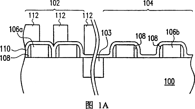
[0029] 2A to 2F are cross-sectional views of the fabrication process of selective local salicide according to an embodiment of the present invention.

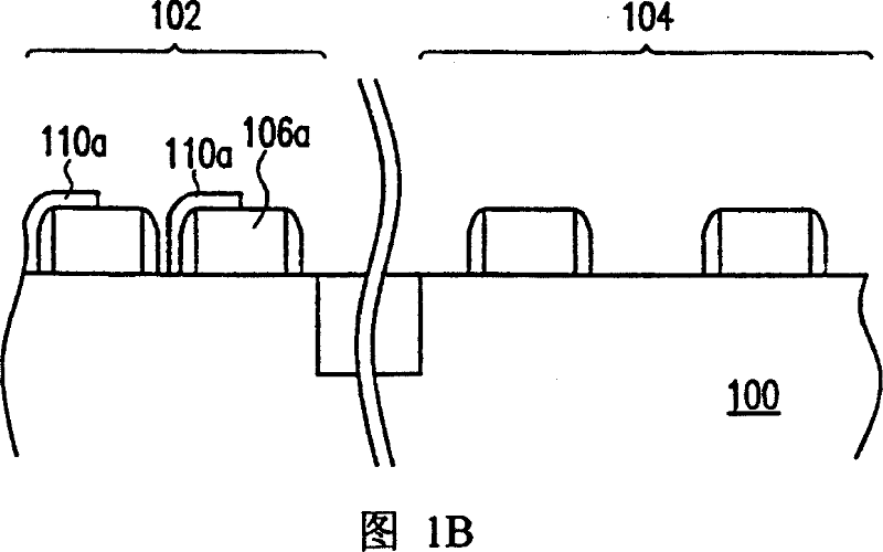
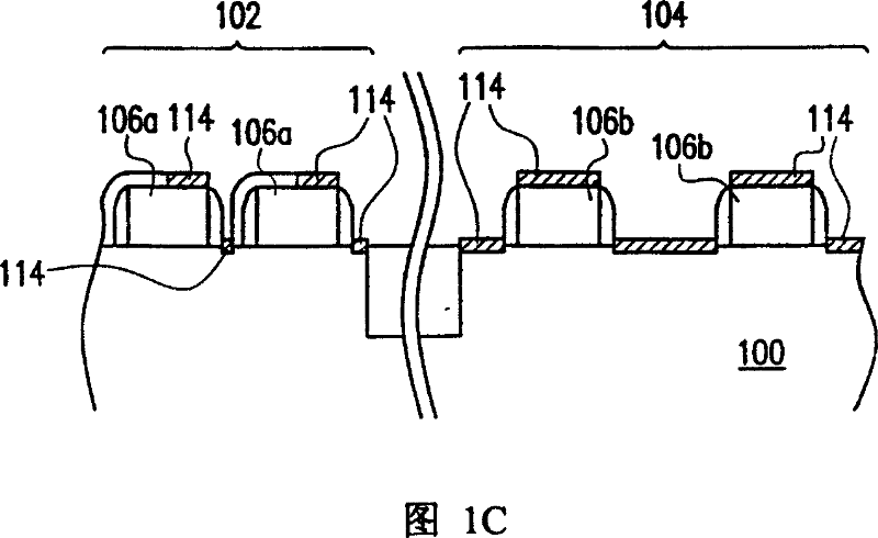
[0030] Referring to FIG. 2A , firstly, a substrate 200 divided into a memory cell area 202 and a logic circuit area 204 by an isolation area 203 is provided. Then, a plurality of gates 206 a, 260 b are formed on the substrate 200 , and the gap between the gates 206 a of the memory cell region 202 is narrower than that of the gates 206 b of the logic circuit region 204 . In addition, a spacer 208 is formed on the sidewalls of the gates 206a and 206b.

[0031] Next, referring to FIG. 2B , a conformal first barrier layer 210 is formed on the substrate 200, such as a photoresist protection oxide layer (Resist Protect Oxide, PRO for short), and its material is such as silicon oxide to cover the memory cell area. 202 and logic circuit area 204 . The first barrier layer 210 on the memory cell area 202 can reduce the width of the gap...


PUM


Abstract

A process for preparing the selectively local self-alignment silicide includes covering a common barrier layer on the memory unit region with more narrow gaps, generating another barrier layer on substrate to cover the memory unit region and logic circuit region, and back etchnig to expose the polysilicon gate and silicon substrate, where said self-alignment silicide is formed, and selectively generating the local self-alignment silicide.

Description

technical field [0001] The present invention relates to a method for fabricating self-aligned silicide (Salicide for short), and in particular to a method for fabricating a Selectivity partial (Partial) self-aligned silicide. Background technique [0002] In deep sub-micron integrated circuit technology, due to the gradual reduction of line width, contact area and junction depth, in order to effectively improve the working quality of components, reduce resistance and reduce signal transmission caused by resistance and capacitance Delay (RC Delay), so when making the gate, a layer of metal silicide (Silicide) is formed on the polycrystalline gate. [0003] Since no development is required in the metal silicide process, the metal silicide produced by this type of process is also called a self-aligned metal silicide. 1A to 1C are cross-sectional views of a known manufacturing process for selective local formation of salicide. [0004] Please refer to FIG. 1A, a memory cell re...

Claims


Application Information

Patent Timeline
Patent Type & Authority Patents(China)
IPC IPC(8): H01L21/82H01L21/283H01L21/3205
Inventor 梁明中蔡信谊
Owner MACRONIX INT CO LTD
Why Eureka
Try Eureka