
Flash memory unit and mfg. method

A storage unit and manufacturing method technology, applied in information storage, static memory, read-only memory, etc., can solve the problems of increasing the complexity of the back-end manufacturing process, the difficulty of the manufacturing process, and the large opening of the contact window, so as to increase the margin of the manufacturing process degree, simplify the manufacturing process, and improve the efficiency of components

Inactive Publication Date: 2007-12-19
POWERCHIP SEMICON CORP
View PDF4 Cites 0 Cited by
  • Summary
  • Abstract
  • Description
  • Claims
  • Application Information

AI Technical Summary

Problems solved by technology

Since the aspect ratio of the opening of the contact window is very large, and two different materials (silicon oxide and silicon) need to be etched, it is difficult to control the depth of the opening of the contact window, which increases the difficulty of the manufacturing process.
Moreover, in the back-end manufacturing process, since the contact windows in the memory cell area and the contact windows in the peripheral circuit area must be formed separately, the complexity of the back-end manufacturing process will also be increased.

Method used


Image

  • Flash memory unit and mfg. method
  • Flash memory unit and mfg. method
  • Flash memory unit and mfg. method

Examples


Embodiment Construction

[0039] In order to make the above-mentioned purposes, features, and advantages of the present invention more obvious and understandable, a preferred embodiment is specifically cited below, and in conjunction with the accompanying drawings, the detailed description is as follows:

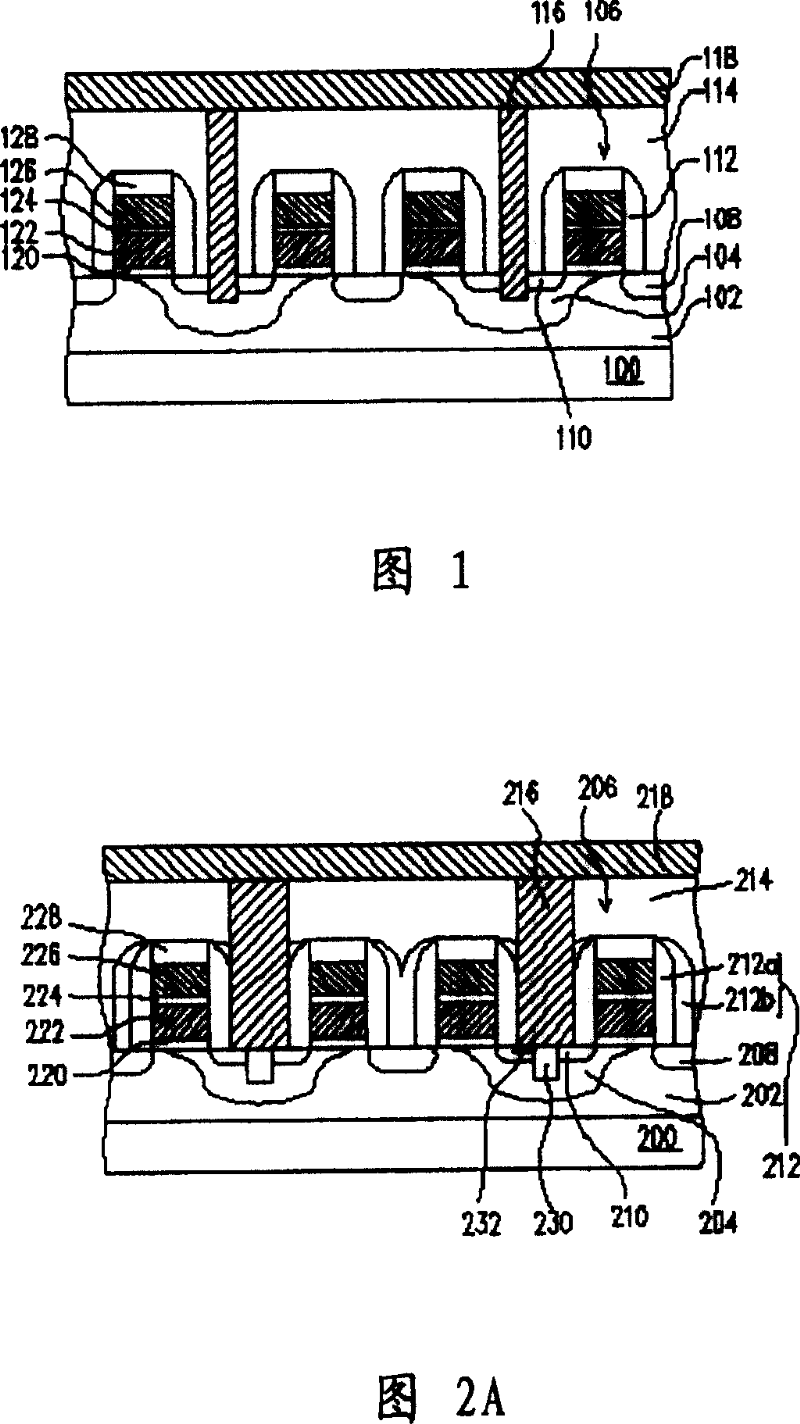
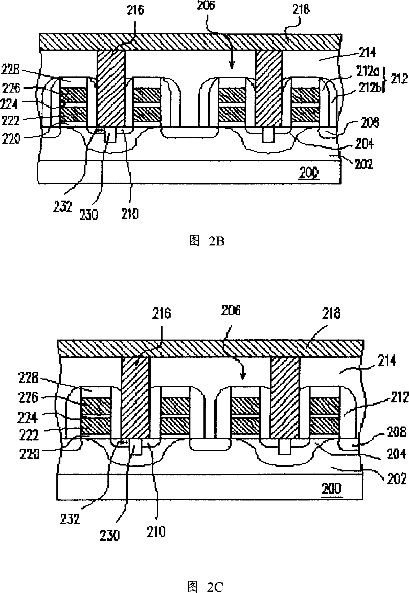
[0040] FIG. 2A is a cross-sectional view illustrating a structure of a flash memory unit according to a preferred embodiment of the present invention. FIG. 2B and FIG. 2C are cross-sectional views illustrating structures of flash memory cells according to other embodiments of the present invention. In FIG. 2B and FIG. 2C , components that are the same as those in FIG. 2A are given the same reference numerals, and detailed descriptions thereof are omitted.

[0041]Please refer to FIG. 2A, the flash memory of the present invention is composed of a p-type substrate 200, a deep n-type well region 202, a p-type pocket doped region 204, a stacked gate structure 206, a source region 208, a drain region 210,...


PUM


Abstract

The quick flash memory comprises following parts: P type substrate, deep N type trap area setup on P type substrate, stack grid structure comprising oxide layer through tunnel, floating grid, dielectric layer in grid poles, control grid pole and top layer in sequence on P type substrate, source pole and drain pole positioned at two sides of the said stack grid structure, gap wall at side of the stack grid structure, P type pocket dope area extended from drain area to position near to source area and under lower trap of the stack grid structure, P type dope area through the drain area and junctions on P type pocket dope area, and contact window above the drain area and connected to P type dope area electrically.

Description

technical field [0001] The invention relates to a non-volatile memory (Non-Volatile Memory, NVM) component, in particular to a flash memory unit and a manufacturing method thereof. Background technique [0002] Flash memory components have the advantages of being able to store, read, and erase data multiple times, and the stored data will not disappear after power failure, so it has become a widely used in personal computers and electronic devices. A non-volatile memory component. [0003] A typical flash memory component uses doped polysilicon to make a floating gate (Floating Gate) and a control gate (Control Gate). Moreover, the control gate is directly arranged on the floating gate, the floating gate and the control gate are separated by a dielectric layer, and the floating gate and the substrate are separated by a tunnel oxide layer (Tunnel Oxide), forming The so-called stacked gate flash memory cell. [0004] Please refer to FIG. 1 for a schematic structural diagram...

Claims


Application Information

Patent Timeline
Patent Type & Authority Patents(China)
IPC IPC(8): H01L27/115H01L27/105H01L21/8239H01L21/8247G11C16/04
Inventor 王进忠杜建志宋达徐震球
Owner POWERCHIP SEMICON CORP
Learn More