Manufacturing process of self-aligned silicide barrier layer

A technology of self-aligned silicide and manufacturing process, which is applied in semiconductor/solid-state device manufacturing, electrical components, circuits, etc., and can solve problems such as reducing leakage current and filling capacity

Active Publication Date: 2008-12-10
SHANGHAI HUAHONG GRACE SEMICON MFG CORP
View PDF7 Cites 0 Cited by
  • Summary
  • Abstract
  • Description
  • Claims
  • Application Information

AI Technical Summary

Problems solved by technology

[0004] The technical problem to be solved by the present invention is to provide a method for manufacturing a self-aligned silicide barrier layer, which can solve the problem of the filling capacity of the self-aligned silicide barrier layer between polysilicon lines, and effectively overcome the pinhole phenomenon. Reduce leakage current

Method used


Image

  • Manufacturing process of self-aligned silicide barrier layer
  • Manufacturing process of self-aligned silicide barrier layer
  • Manufacturing process of self-aligned silicide barrier layer

Examples


Embodiment Construction

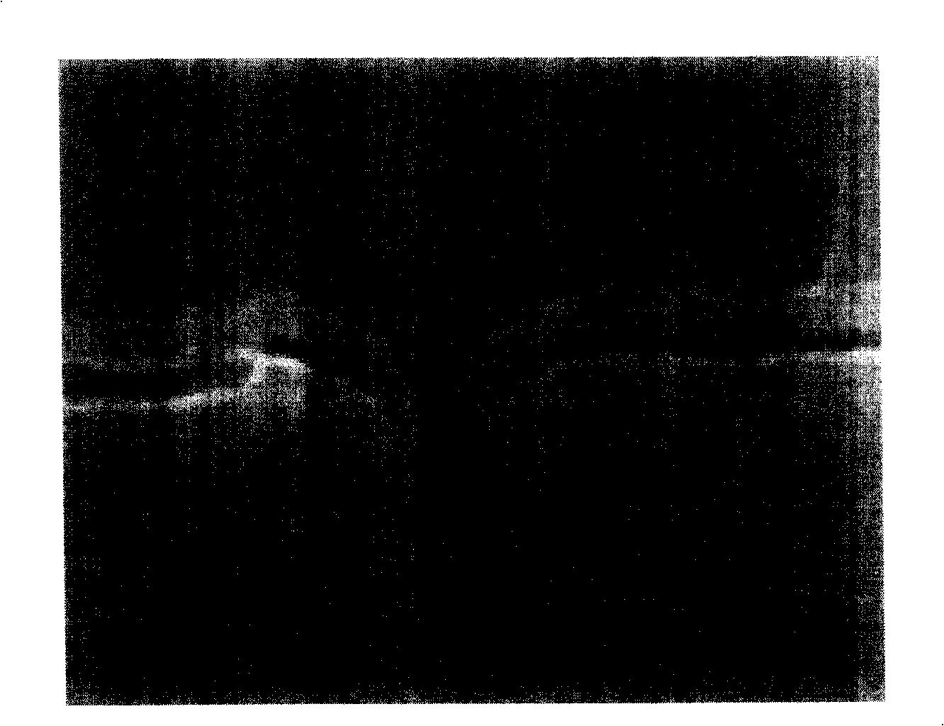
[0012] Such as image 3 As shown, the existing salicide barrier layer growth process method includes the following steps: adopt PECVD (plasma enhanced chemical vapor deposition) to grow a layer of silicon dioxide, glue, salicide Blocking layer (SAB) mask plate photomask, perform HF (hydrofluoric acid) etching, and grow self-aligned refractory metal silicide (Salicide) layer.

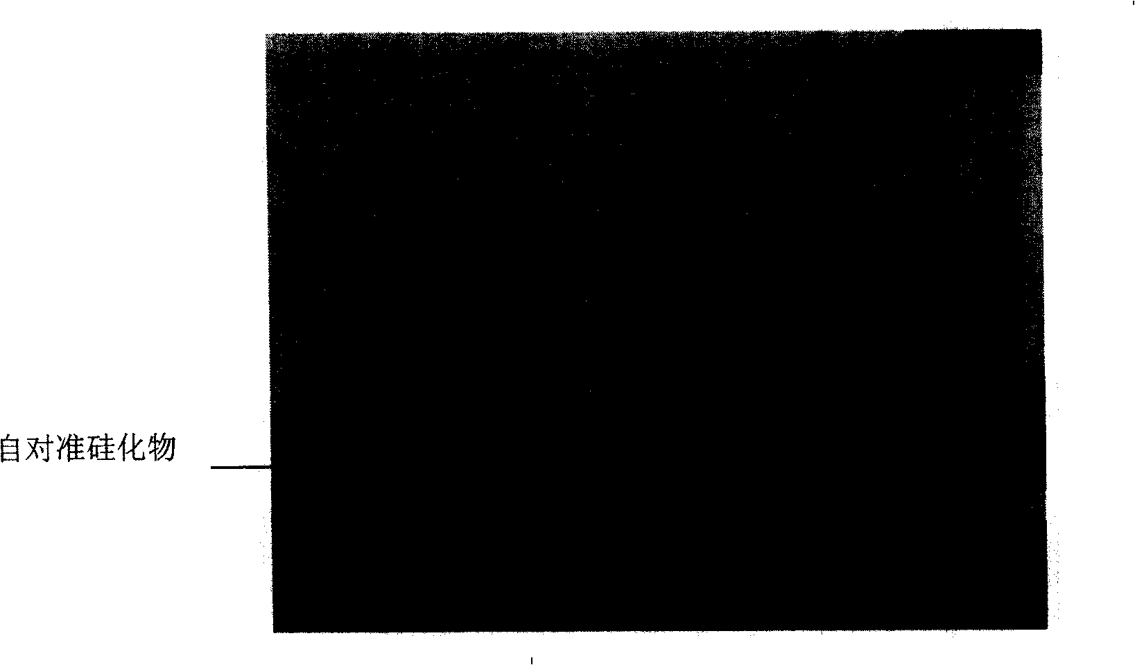
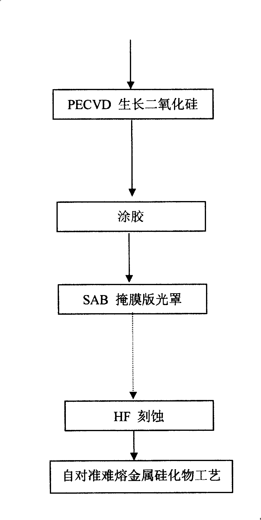
[0013] The self-aligned silicide barrier layer growth process flow of the present invention is as follows Figure 4 As shown, it includes the following steps: growing the first layer of silicon dioxide by CVD method, regrowing the second layer of silicon dioxide on the first layer of silicon dioxide by HDP method, coating, SAB mask plate photomask, Perform HF etching and grow the Salicide layer.

[0014] The process flow of the present invention is the same as the existing process flow. At first, a layer of silicon dioxide is grown by CVD, but the first layer of silicon dioxide grown by the method of t...


PUM


Abstract

The invention discloses a method for manufacturing a self-aligned silicide barrier layer. First, a first layer of silicon dioxide is grown by CVD, and then a second layer of silicon dioxide is grown on the first layer of silicon dioxide by HDP. silicon. The invention can solve the problem of the filling ability of the self-aligned silicide barrier layer between the polysilicon lines, effectively overcome the pinhole phenomenon, and achieve the purpose of reducing the leakage current.

Description

technical field [0001] The invention relates to a manufacturing process method of a semiconductor integrated circuit, in particular to a manufacturing process method of a self-aligned silicide barrier layer. Background technique [0002] With the development of integrated circuits, the polysilicon line width and the spacing between line widths are becoming narrower and narrower, which has more and more implications for the filling ability of salicide blocks between polysilicon lines. Come higher demands. When the filling capacity is insufficient, such as figure 1 In the case shown in , voids are created between polysilicon lines due to insufficient filling capability. [0003] At the same time, due to the consideration of the filling ability, it is required that the grown salicide barrier layer should be as thin as possible, but this will inevitably cause pinholes, which will affect the device. Such as figure 2 As shown, the pinhole phenomenon due to the formation of th...

Claims


Application Information

Patent Timeline
Patent Type & Authority Patents(China)
IPC IPC(8): H01L21/316
Inventor 陈华伦周贯宇
Owner SHANGHAI HUAHONG GRACE SEMICON MFG CORP
Why Eureka
Try Eureka