A making method for thermal sediment of GaAs single-chip microwave integration circuit power amplifier

A technology of microwave integrated circuits and power amplifiers, which is applied in the manufacture of circuits, electric solid-state devices, semiconductor/solid-state devices, etc. , Solve the phenomenon of bond fracture and the effect of small loss angle

Inactive Publication Date: 2009-01-07
SHENYANG ZHONGKE MICROELECTRONICS
View PDF3 Cites 2 Cited by
  • Summary
  • Abstract
  • Description
  • Claims
  • Application Information

AI Technical Summary

Problems solved by technology

However, due to the large difference between the thermal expansion coefficient of the bonding material and the ceramic substrate itself and the GaAs chip in repeated tests, the ceramic substrate and the GaAs chip are prone to breakage, which makes the reliability of the chip work unfavorable. to guarantee

Method used


Image

  • A making method for thermal sediment of GaAs single-chip microwave integration circuit power amplifier
  • A making method for thermal sediment of GaAs single-chip microwave integration circuit power amplifier
  • A making method for thermal sediment of GaAs single-chip microwave integration circuit power amplifier

Examples


Embodiment

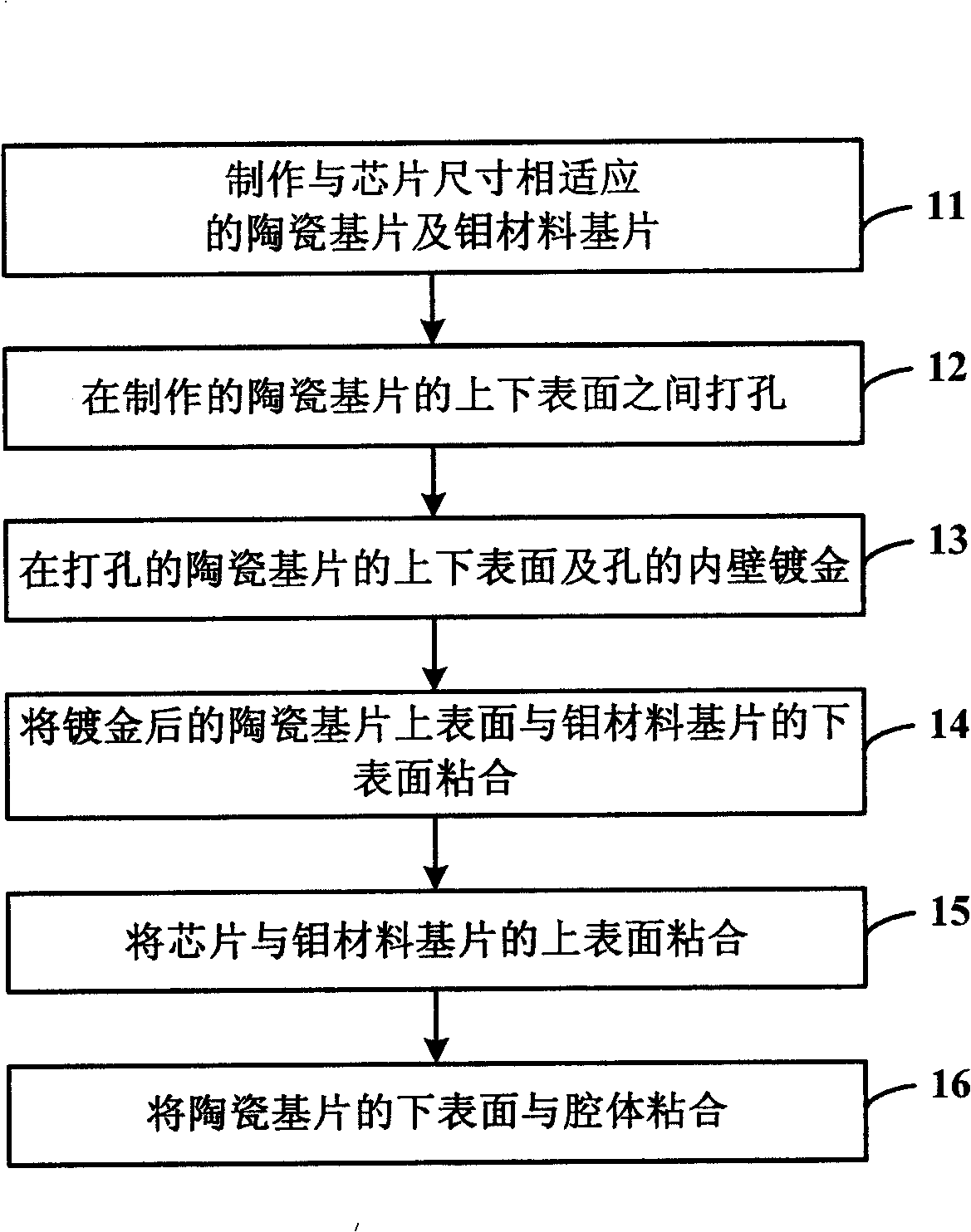
[0063] Such as figure 2 as shown, figure 2 A flow chart of a method for making a GaAs MMIC power amplifier heat sink according to an embodiment of the present invention, the method includes the following steps:

[0064] Step 21: making a ceramic substrate with the same length and width as the chip and having a thickness calculated according to the operating frequency band of the chip, and making a molybdenum material substrate with the same length, width and thickness as the chip;

[0065] The ceramic substrate is Al 2 o 3 A ceramic substrate with a content greater than or equal to 99%, or an aluminum nitride ceramic substrate; the molybdenum material substrate is a pure molybdenum material substrate;

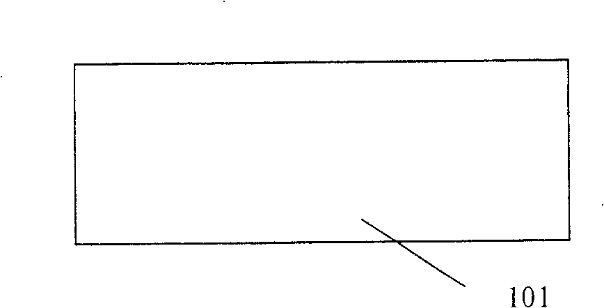
[0066] In this step, the prepared ceramic substrate 201 is as diagram 2-1 as shown, diagram 2-1 It is a schematic diagram of a ceramic substrate 201 fabricated according to an embodiment of the present invention.

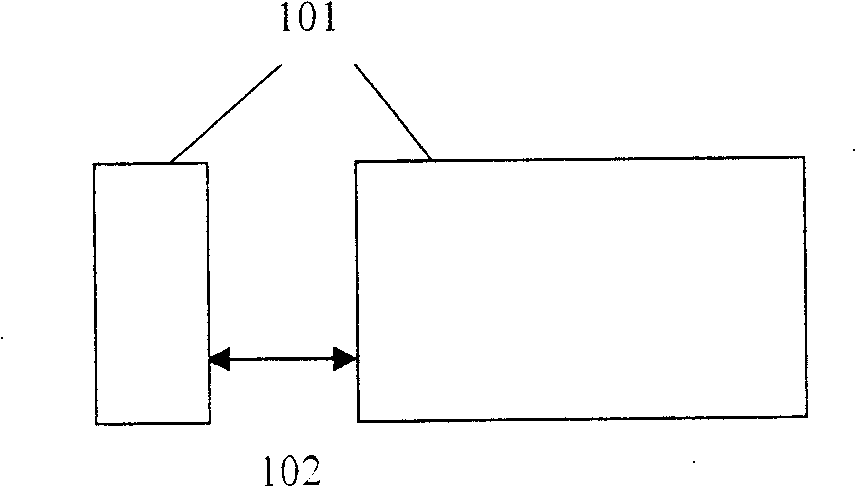
[0067] Step 22: Drill a through hole 202 with a diame...


PUM

PropertyMeasurementUnit
thicknessaaaaaaaaaa

Abstract

The utility model discloses a manufacture method of heat sink of the GaAs MMIC power amplifier, comprising: A, a ceramic substrate surface and a substrate surface made of molybdenum matched with the size of a chip are made; B, holes are punched between an upper surface and a lower surface of the ceramic substrate surface; C, gold is plated on the upper surface and the lower surface of the punched ceramic substrate surface and the inner wall of the holes; D, the upper surface of the plated ceramic substrate surface is bonded with the lower surface of the substrate surface made of molybdenum; E, the chip is bonded with the upper surface of the substrate surface made of molybdenum; F, the lower surface of the substrate surface made of molybdenum is bonded a cavity, then the manufacture of the heat sink is completed. With the ceramic substrate surface and the substrate surface made of molybdenum, the utility model can avoid the fracture easily caused by bonding the chip to the ceramic substrate surface directly due to the different thermal expansion property of the two materials, solving the problems of the chip single-valve overburning caused by the bad heat conductivity of the GaAs chip and the heat dissipating not timely, so as to solve the adherence fracture of the GaAs chip and enhance the reliability of the chip.

Description

technical field [0001] The invention relates to the technical field of microelectronics power amplifier testing, in particular to a method for manufacturing a heat sink of a gallium arsenide monolithic microwave integrated circuit (GaAs MMIC) power amplifier. Background technique [0002] GaAs MMIC power amplifier heat sink is mainly used for heat dissipation and grounding of GaAs MMIC power amplifier. From the perspective of heat transfer, the heat sink is made by installing a heat exchange component on the MMIC, which has a heat exchange contact with the MMIC, and passes through the heat exchange component to transfer heat to the cavity; from an electrical point of view, it can play a role To a good grounding, so that the contact part of the MMIC chip to the ground will not produce crosstalk and affect the work of the chip. [0003] When the GaAs MMIC power amplifier is working, due to the repeated heating of the GaAs chip and the heat sink material, the GaAs MMIC power a...

Claims


Application Information

Patent Timeline
Patent Type & Authority Patents(China)
IPC IPC(8): H01L21/48H01L23/373
Inventor 朱旻张海英刘训春
Owner SHENYANG ZHONGKE MICROELECTRONICS
Why Eureka
Try Eureka