

Phosphor thin film, its production method and EL panel
A technology of phosphors and thin films, which is applied in the direction of discharge tube phosphor screens, chemical instruments and methods, light sources, etc., can solve the problems of increased panel manufacturing costs, complicated manufacturing processes, and inability to be practically applied, and achieves the effect of reducing costs.
- Summary
- Abstract
- Description
- Claims
- Application Information
AI Technical Summary
Problems solved by technology
Method used
Image

Examples
Embodiment 1
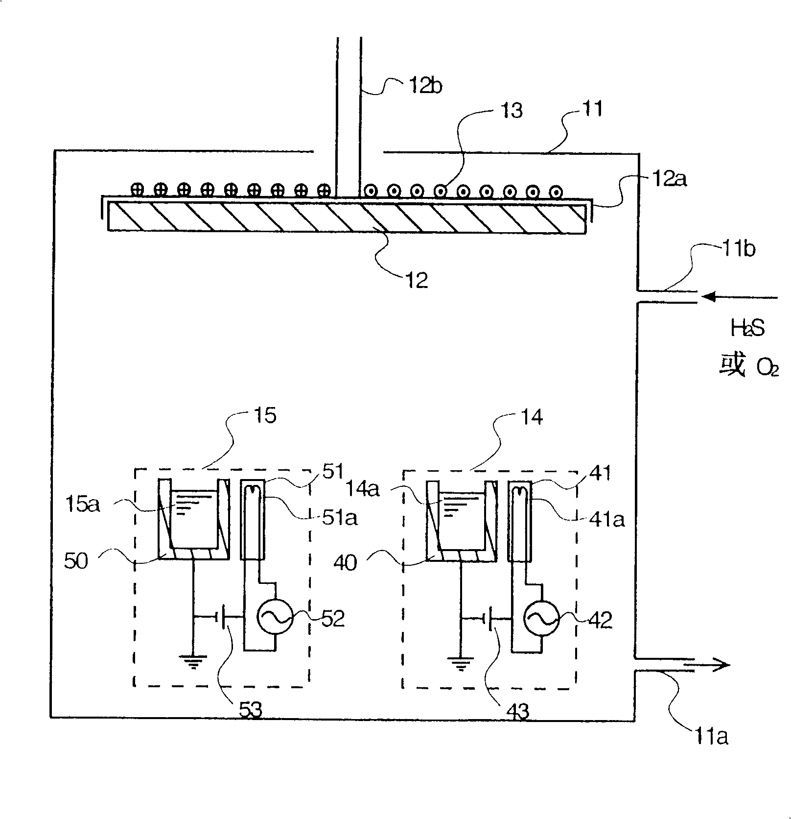
[0111] An EL element using the phosphor thin film of the present invention was produced. The substrate and thick film insulating layer use the same material BaTiO 3 Class dielectric material (dielectric constant 5000), the lower electrode uses Pd electrode. First, a green sheet of the substrate is produced, and the lower electrode and the thick-film dielectric layer are screen-printed thereon, and then the whole is sintered. Next, the surface was ground to obtain a substrate having a 30 μm thick thick-film dielectric layer. Furthermore, a 400nm thick BaTiO was formed on it by sputtering 3 The film was annealed in air at 700°C to form a composite substrate.
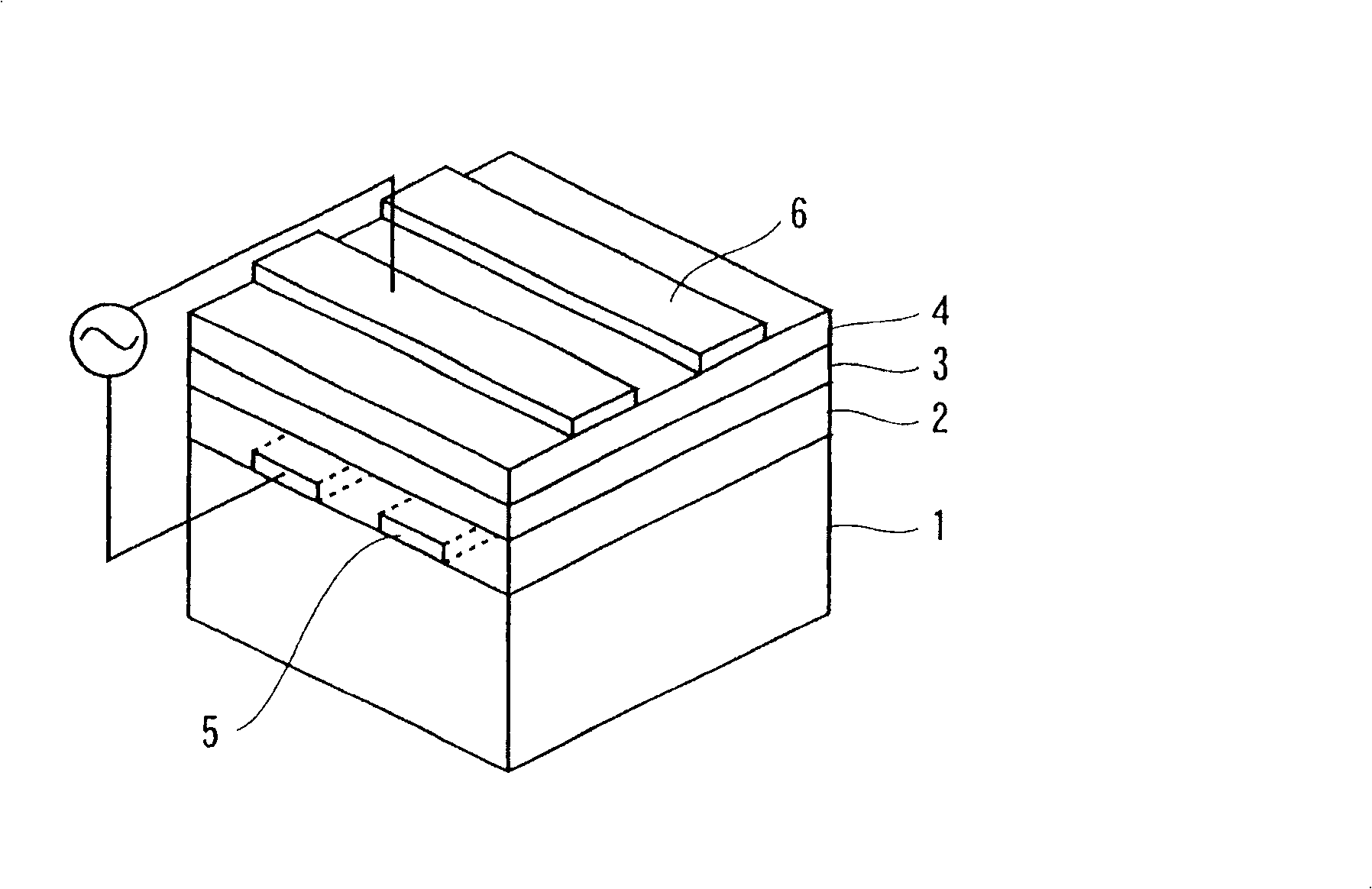
[0112] Formed on the composite substrate made of Al 2 o 3 Film (50nm thick) / ZnS film (200nm thick) / phosphor thin film (300nm thick) / ZnS film (200nm thick) / Al 2 o 3 A laminated structure composed of films (50 nm thick). The purpose of each film provided on both sides of the phosphor film is to make the EL element em...
Embodiment 2
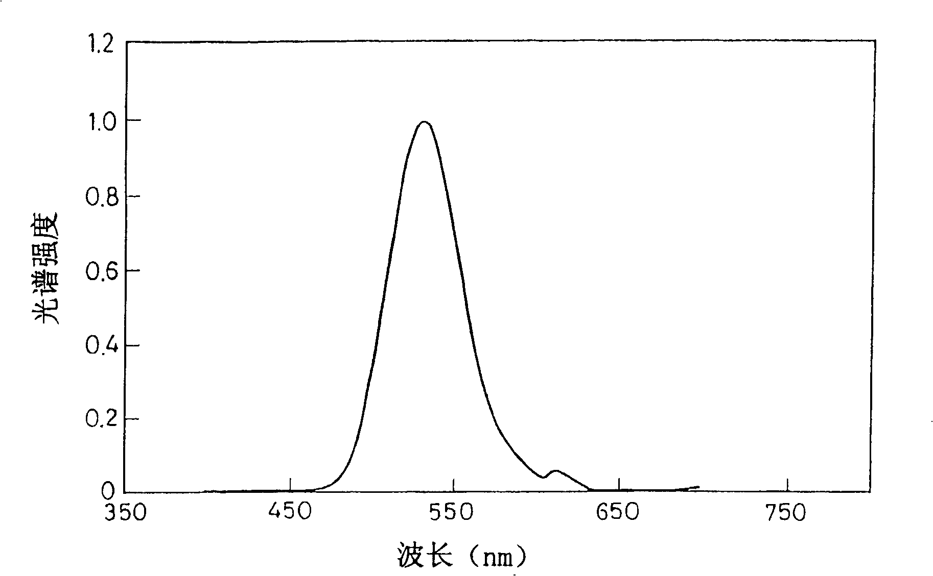
[0128] In Example 1, Tb was used instead of Eu to obtain a luminance of 53cd / m 2 green glow.
Embodiment 3
[0130] In Example 1, one or two or more of Mg, Ca, and Ba were used instead of Sr, or together with Sr, and almost the same results were obtained. In this case, a turquoise glow is obtained.
[0131] In addition, in the phosphor thin films formed respectively in Examples 2 to 3 above, y / x in the aforementioned composition formula is in the range of 2.2 to 3.0, z / (w+z) is in the range of 0.13 to 0.33, and (x +3y / 2) / (z+w) is in the range of 0.9 to 1.1.
PUM
| Property | Measurement | Unit |
|---|---|---|
| electrical resistivity | aaaaa | aaaaa |
| thickness | aaaaa | aaaaa |
| luminance | aaaaa | aaaaa |
Abstract
Description
Claims
Application Information