V type coupling cavity wavelength switchable semiconductor laser

A technology of lasers and semiconductors, applied in the structure of semiconductor lasers, optical waveguide semiconductors, lasers, etc., can solve the problems of poor single-mode selection performance, and achieve the effect of low cost and high side mode suppression ratio

Active Publication Date: 2009-02-18
HANGZHOU LIGHTIP TECH CO LTD
View PDF5 Cites 8 Cited by
  • Summary
  • Abstract
  • Description
  • Claims
  • Application Information

AI Technical Summary

Problems solved by technology

This Y-shaped coupled cavity structure has the advantages of easy monolithic integration, no need for deep vertical etching of rectangular grooves, and low manufacturing difficulty. However, its single-mode selectivity is very poor, and the threshold gain coefficients of the main mode and the first-order side mode are poor. Only 1cm for a 450 micron long laser -1 About 10cm compared to the typical value of the general distributed feedback (DFB) laser -1 above

Method used


Image

  • V type coupling cavity wavelength switchable semiconductor laser
  • V type coupling cavity wavelength switchable semiconductor laser
  • V type coupling cavity wavelength switchable semiconductor laser

Examples


Embodiment Construction

[0048] The present invention will be described in detail below according to the drawings and embodiments.

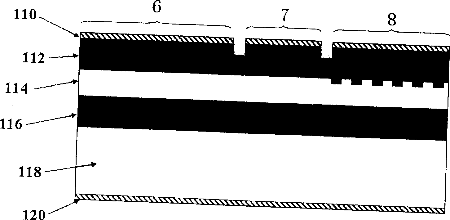
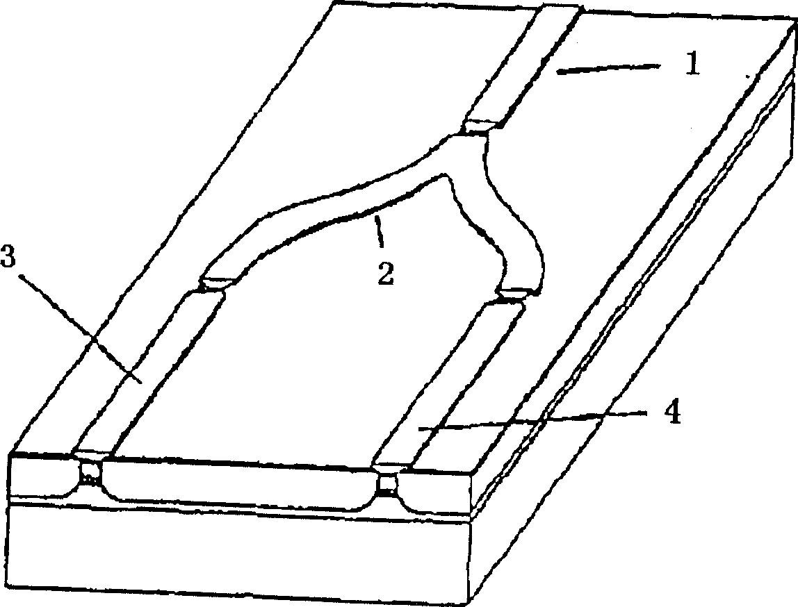
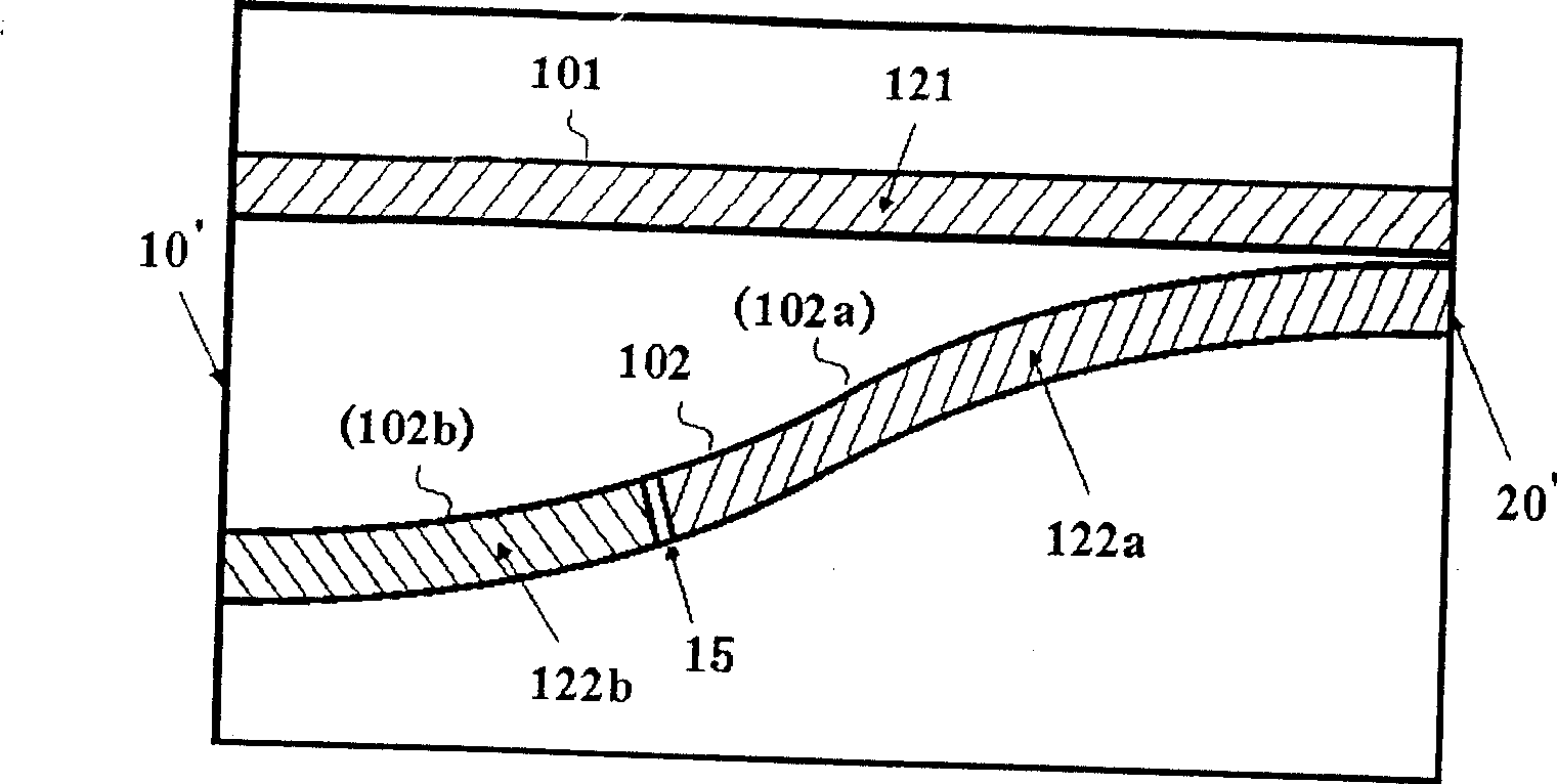
[0049] image 3 It is a schematic diagram of the first embodiment of the monolithic integrated wavelength variable V-coupled cavity laser of the present invention, which includes two optical waveguide arms (respectively optical waveguides 101 and 102 in the figure), arranged side by side on the semiconductor chip Make a V shape. The two optical waveguides are close together at one end (closed end), but far apart at the other end (open end). There is a reflective element at both ends of each optical waveguide, which can be a cleavage reflective surface (respectively image 3 The end face 10' and the end face 20') or rectangular deeply etched grooves (such as 10 and 20 in Figures 14, 16, 17 and 18). Each optical waveguide and the reflective elements at its ends form a Fabry-Perot cavity. Near the end face 20', because the two waveguides are very close or in contact, th...


PUM


Abstract

The invention discloses a V-type coupling cavity wavelength switchable semiconductor laser, comprising two optical resonant cavities, each comprising a segment of light waveguide and partial reflecting elements at the two ends; the two segments of light waveguides are arranged on a chip to form a V shape, there is no coupling at the opening end but there is a certain cross coupling at the closed end to make the laser have optimum single-mode selectivity; the first optical resonant cavity has a fixed optical length to make its resonant frequency be on a series of independent equidistant channels; the second optical resonant cavity has a certain length difference from the first one, and by changing effective refractivity of partial waveguides in the second optical resonant cavity, it can make the laser wavelengths mutually switched on a series of channels determined by the first optical resonant cavity. And the laser can further comprise one or two branch couplers or directional couplers added outside the cavity to improve coupling efficiency of external devices, and providing added modulating or space switching functions.

Description

technical field [0001] The invention relates to a semiconductor laser, in particular to a single-chip integrated wavelength-switchable single-mode semiconductor laser. Background technique [0002] Broadband tunable lasers are widely used in metropolitan area network and long-distance telecommunication. In addition to being used as a replacement light source, which can reduce inventory numbers and costs, it can also provide the possibility to design more efficient and flexible network structures. For example, the combination of tunable lasers and wavelength routers can realize spatial optical switches and reconfigurable optical add-drop multiplexing functions. [0003] Compared with external cavity tunable lasers composed of separate components, monolithic integrated semiconductor tunable lasers have many advantages, such as compact structure, low cost, and higher reliability because there are no moving parts. Traditional monolithic integrated tunable semiconductor lasers ...

Claims


Application Information

Patent Timeline
Patent Type & Authority Patents(China)
IPC IPC(8): H01S5/10H01S5/24H01S5/00
Inventor 何建军
Owner HANGZHOU LIGHTIP TECH CO LTD
Why Eureka
Try Eureka